🛠️ Code to all kernels mentioned in this series is available on GitHub.
This series of blog posts will showcase how one can:
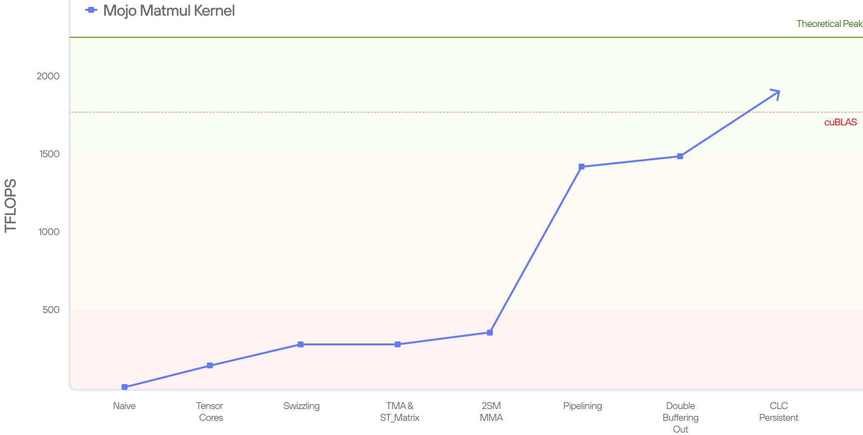
- Write a high-performance GPU kernel on Blackwell that offers performance competitive to that of NVIDIA's cuBLAS implementation.
- Shows how one can leverage Mojo's special features to make the kernel as simple as possible.
It is our hope that this series of blogs serves as the reference worklog for NVIDIA’s Blackwell GPU. While there is prior work on optimizing NVIDIA's Ampere and Hopper generation of GPUs, none currently exist to provide a blueprint for optimizing NVIDIA's Blackwell GPUs.
In Part 1 (this blog post) we cover what a Matrix Multiplication (matmul) is, its importance for LLMs, and why we need to optimize it. Then we explain what a GPU is, GPU history since Ampere, and finally how to write a simple (not super performant) implementation of matmul on a GPU in 4 lines of Mojo.
In part 2, we’ll explain the hardware instructions introduced in Blackwell GPUs, and continue improve on our kernels' performance to make it leverage the new hardware instructions. As we continue through the blog series, we will incrementally leverage new Blackwell features to improve our matmul implementation until the end of the series where we achieve performance that surpasses that of NVIDIA's cuBLAS library.
What is matmul?
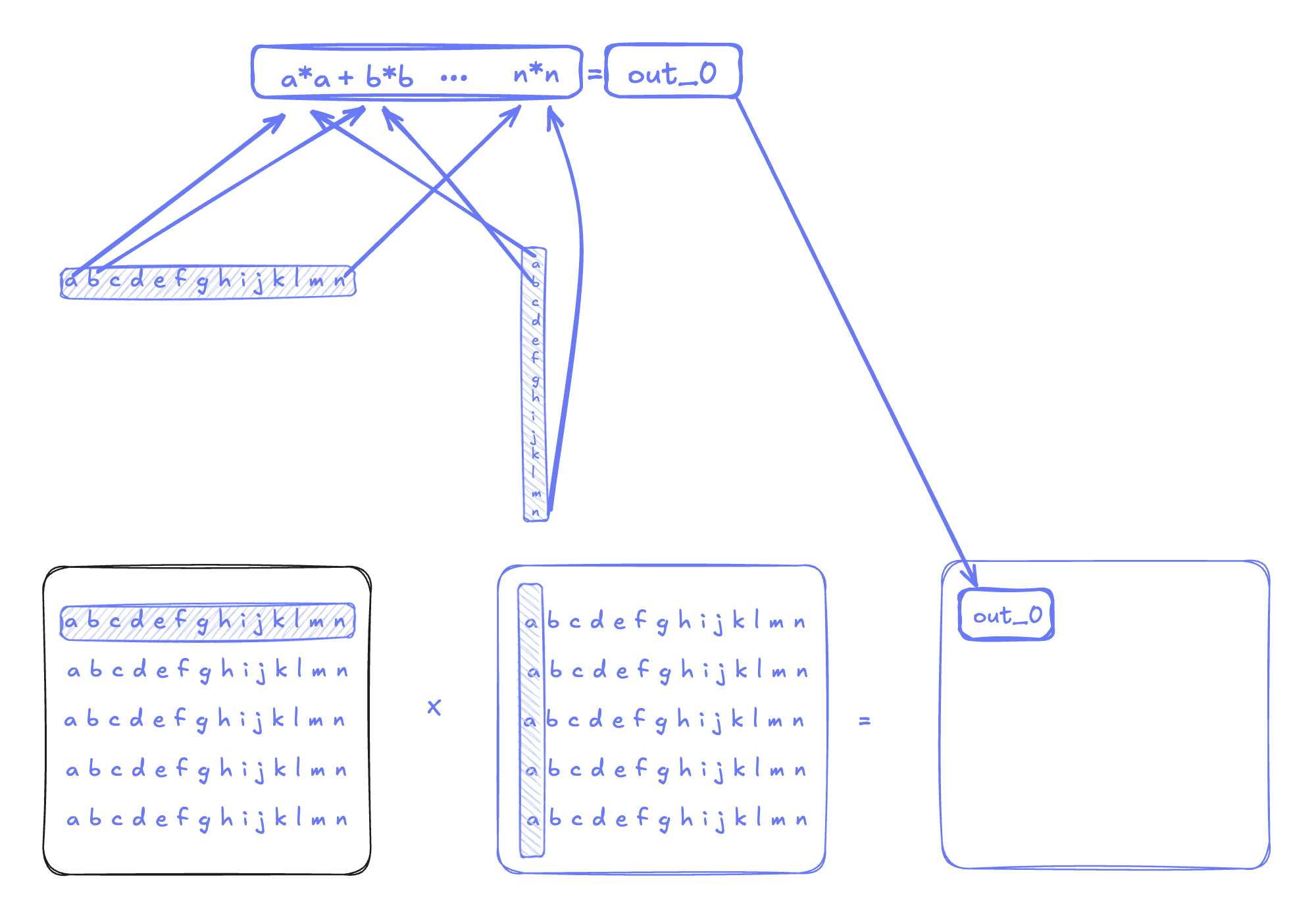
Given two dense matrices A and B of dimensions MxK and KxN respectively, we want to compute the matrix multiplication C = A.B which is defined by
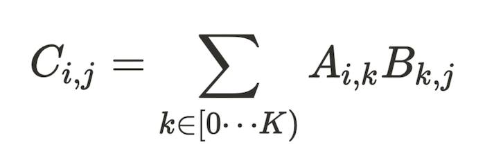
Since matrix multiplication is a core part of linear algebra and presents itself in many areas, there has been extensive research on writing efficient algorithms. Readers who are interested in a deeper background of matmul are encouraged to read our blog post from 2 years ago.
Why Does matmul matter today?
All LLMs, be it Meta's Llama, Alibaba's Qwen, Deepseek, Anthropics' Claude, OpenAI's ChatGPT, or Google's Gemini, utilize matrix multiplications at their core. These matmuls might be disguised under multiple names, for instance, the Multi-Layer Perceptron (MLP), which is sometimes called the Linear layer, is an A.B^T matmul operation. The same is true for Attention, Latent Attention, Mixture of Experts, and so on.
In fact, if we look at a profile from the Llama 8B model using FP8 on 2xB200, we observe that over 83% of the model's runtime is occupied executing some variant of matmul (e.g. linear, attention and MLP layers).
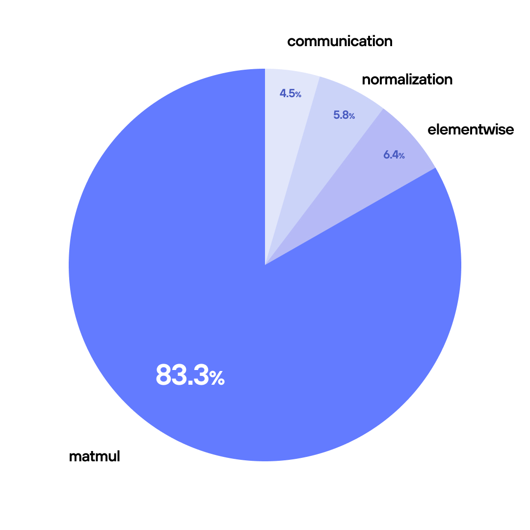
As a result, even a 10% improvement in matmul performance yields around 8% end-to-end speedup. For companies spending hundreds of millions on serving, these optimizations translate directly to millions of dollars in savings.
Why do we care about GPUs?
We will motivate the value of GPUs by looking at matmul. Furthermore, for simplicity, let’s assume both A and B matrices are square, such that:
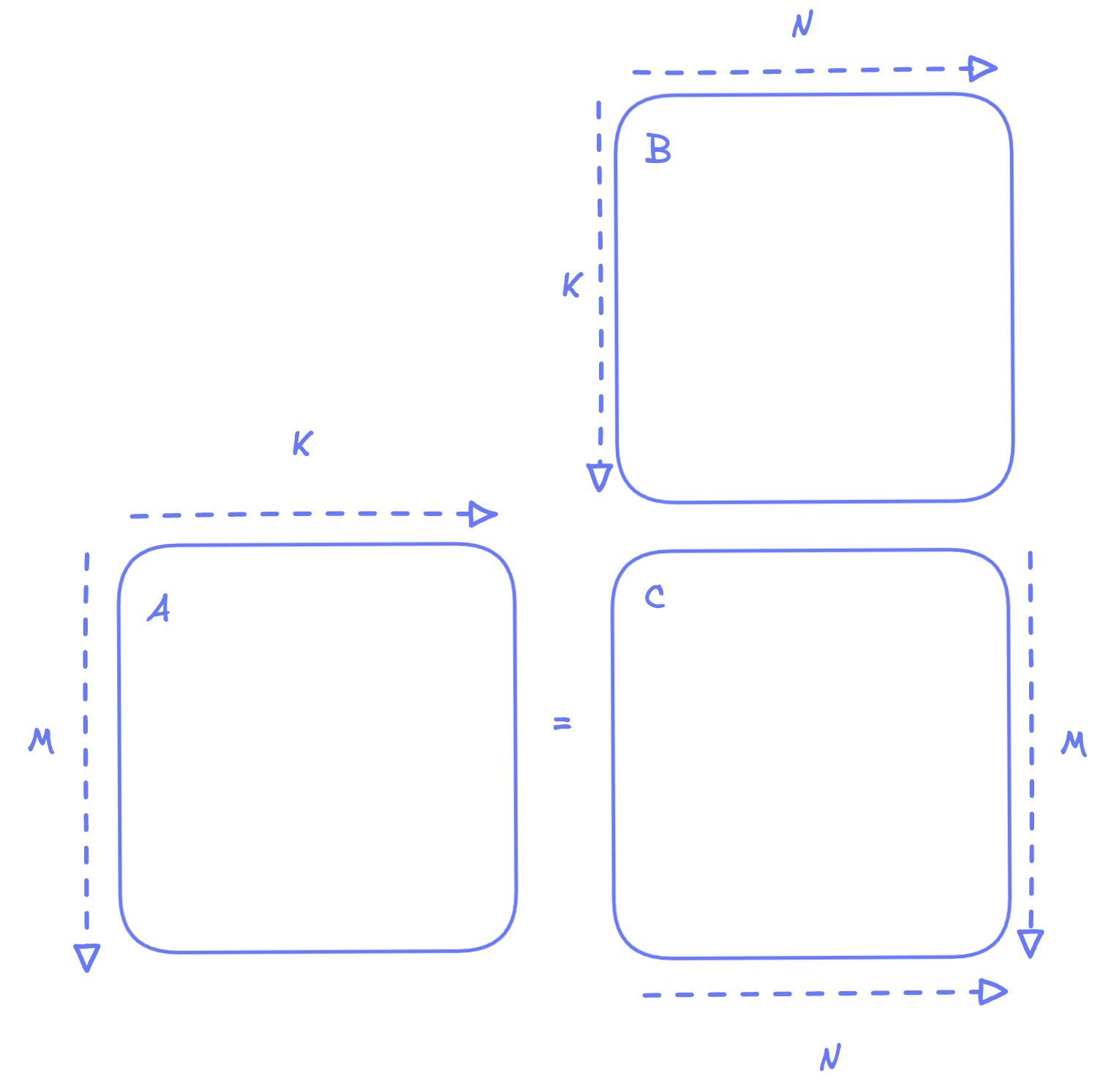
If we want to do the matmul on a CPU, then here’s pseudocode code we’ll have to write:
Essentially the code calculates the inner product across the K dimension for output element.
CPUs are limited to on the order of a few hundred cores (with lower-end CPUs having around 32 cores and high-end models having on the order of 128 cores). GPUs, on the other hand, offer massive parallelism: modern GPUs handle over 100,000 threads simultaneously (B200s can handle up to 151,552 threads), making them the ideal hardware choice for repetitive, data-parallel operations like matrix multiplication.
To accelerate things even further, recent GPUs (since Volta) have a dedicated fast hardware unit for matrix multiply accumulate (MMA) operations called tensor core. While originally Tensor cores were limited to small matmuls (on the order of 16x16x16), the 5th generation tensors cores introduced in Blackwell can perform a large sub-matrix multiplication (up to 256x256x16). This enables the Blackwell GPUs to increase the peak computation throughput.
GPU from the hardware architect perspective?
To understand GPUs better, let's look at how the GPU is organized from a hardware architecture perspective. A GPU, like other Von Neumann architectures, is composed of elements that compute (commonly known as Arithmetic Logical Units or ALUs), and elements that load/store the data for these computations. A GPU will contain several Streaming Multiprocessor (SM), L2 Cache and global memory which are shared among these SMs, and an interconnect to the host device (CPU).
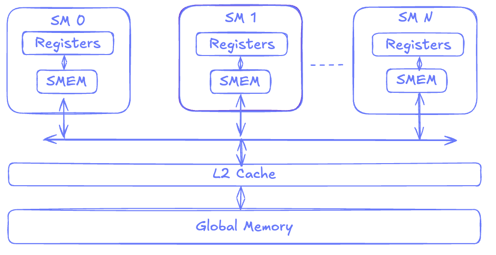
Threads on a GPU are grouped into blocks which are called Thread Blocks or Cooperative Thread Arrays (CTAs). Each of these blocks gets scheduled onto a single SM. Each SM, in turn, access the data via a shared L2 cache which loads data from global memory. The threads in each SM have access to two more memory regions:
- Registers which are local variables and are private to each thread.
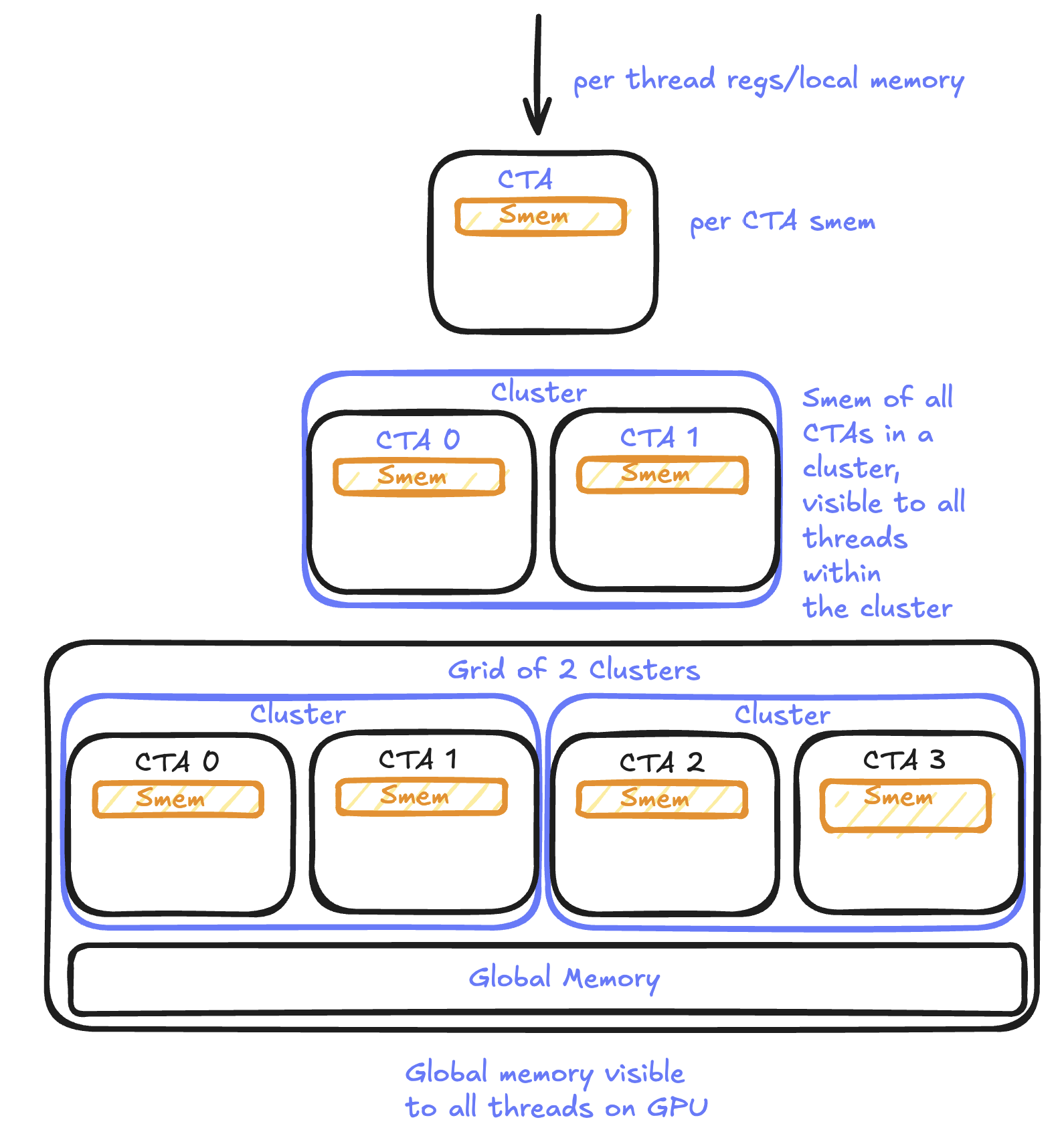
- Shared memory which is visible across threads in an SM. Since Hopper, multiple CTAs can form a cluster and CTAs within the same cluster can access each other's shared memory.
What are Tensor Cores?
While the GPU is an accelerator, within it lies hundreds of mini-accelerators, called Tensor Cores. Tensor Cores are specialized units to perform matrix-multiply-accumulate operations. This is different from the other ALU units which can perform arithmetic computation.
Let's dig into the definition of a Tensor Core by an example. Say we wanted to multiply two matrices together, where the A matrix is MxK in dimension and the B matrix is KxN in dimension:
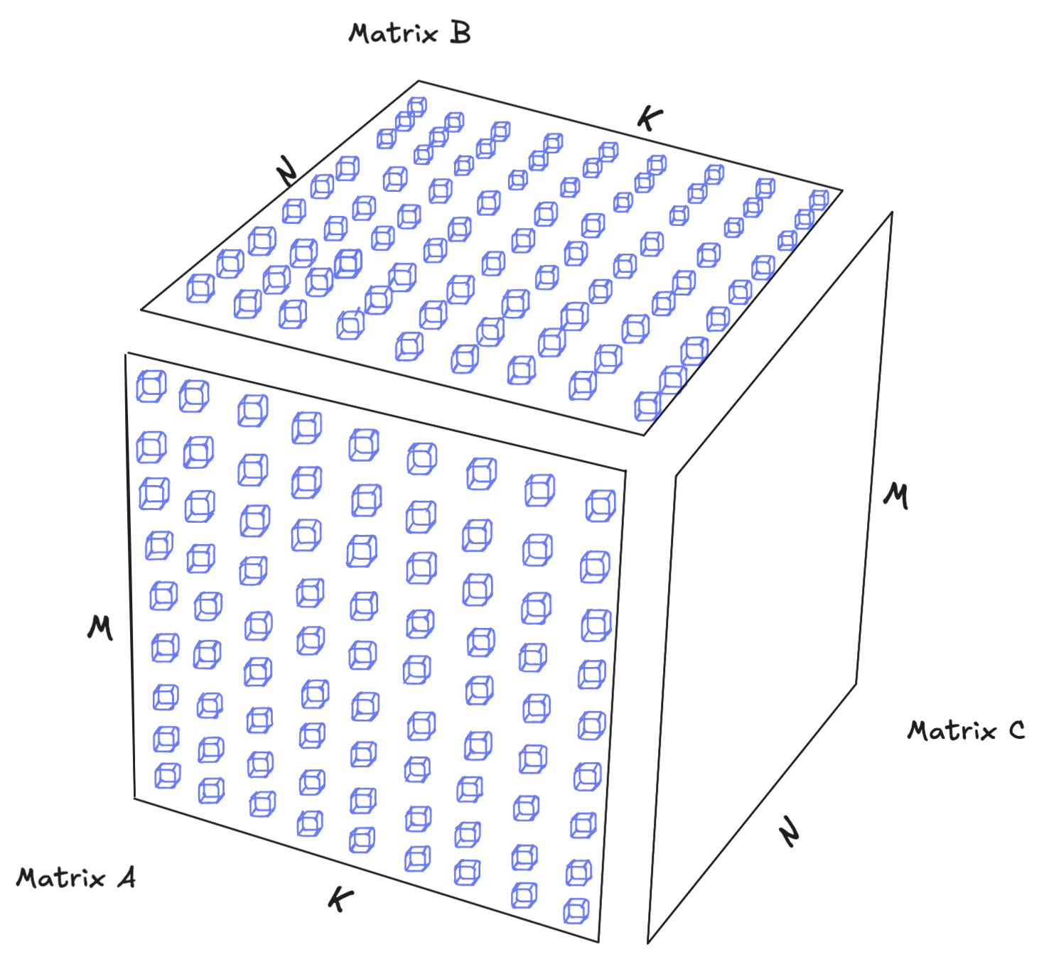
A CUDA core processes a fused multiplication and addition operation at a time, so we are multiplying a single element from matrix A by another element from matrix B and accumulating the value in C per instruction. A Tensor Core, on the other hand, computes an MMA operation (e.g. a 64×128 tile), in a single instruction.
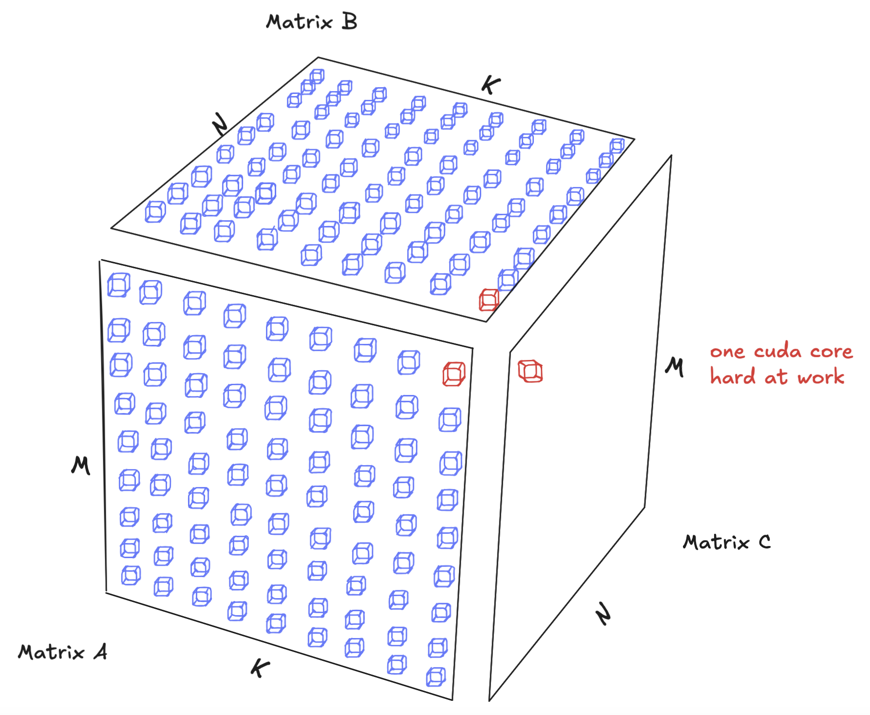
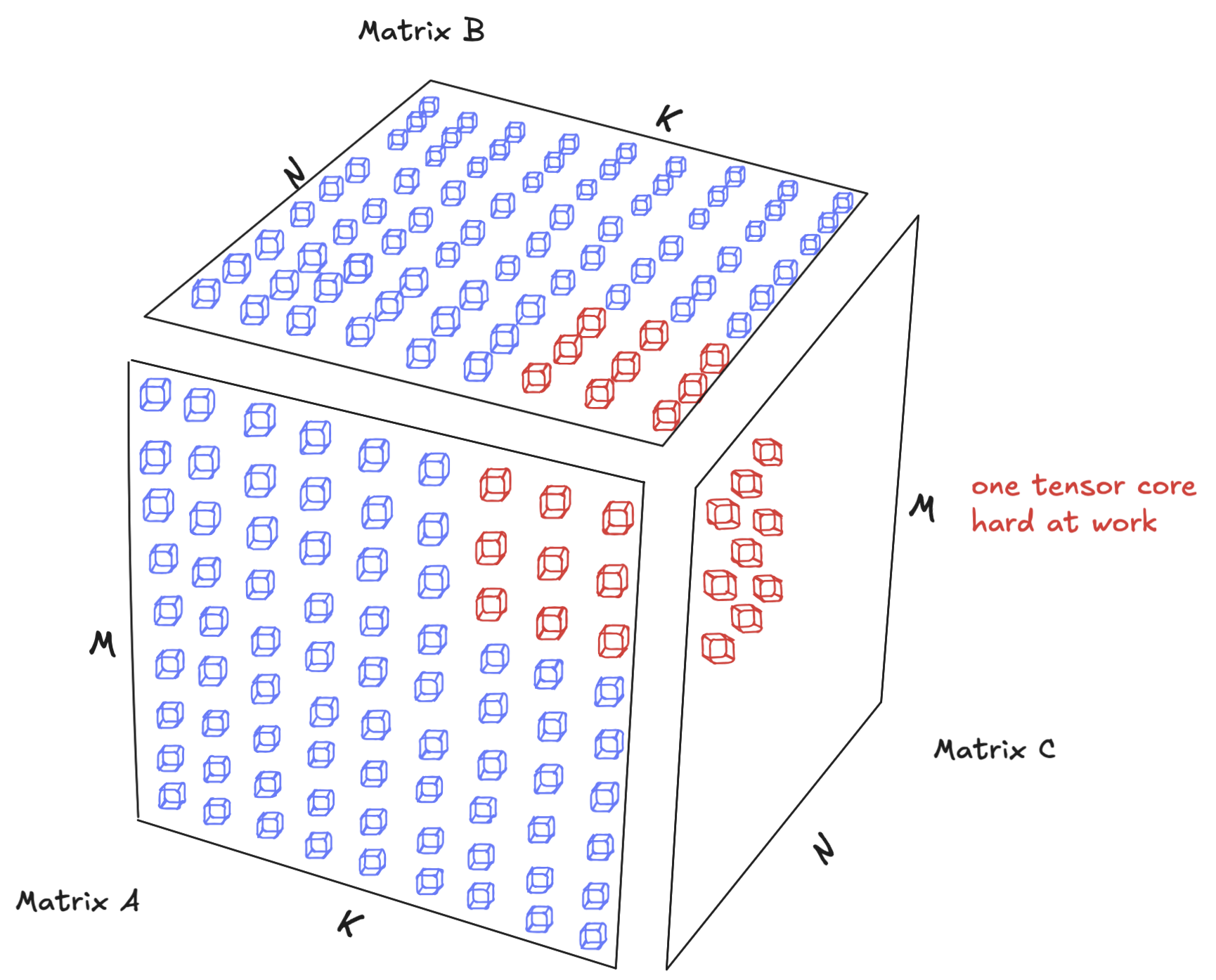
And so it’s natural to see the performance improvement. On a large scale matrix of dimension MxN, we can achieve massive speedup by decomposing the matmul into smaller matmuls (a technique called tiling which will be discussed in a subsequent blog post) and perform the computation using fewer instructions. As a result, we get massive speedups.
The number of Tensor Cores per SM (4 if you’re curious) is not important. This is because when we launch the MMA instructions, the hardware takes care of the partitioning / distribution of the MMA among the tensor cores for us.
In Hopper, the largest WGMMA (Warp Group Matrix Multiply and Accumulate) shape was 64×256×16. WGMMA instructions required four warps (a warp group) and the instruction stored the results in the thread registers. However, Blackwell's 5th generation tensor core (tcgen05) scales up the MMA to 256x256x16 on 2 SMs, and introduces tensor memory, to reduce register usage (which will be covered in subsequent posts).
What is GPU programming?
A detailed description of GPU programming fundamentals is beyond the scope of this blog post. There are many resources that explain the GPU programming paradigm, and a great resource is Mojo GPU Puzzles and the GPU glossary.
As a result of the massive parallelism afforded to by the GPU, one has to think about GPU programming differently. For example, while, in traditional CPU programming we process data sequentially through loops:
With GPUs, we flip this model entirely and process data via threads. So, instead of moving sequentially through data, we map thousands of parallel threads directly onto the data. For our case above, the body of the function would look like:
On GPUs, each thread becomes responsible for computing a single element, eliminating the need for explicit loops. This mental shift from “stepping through data” to “blanketing data with compute” is central to GPU programming. If we think about the Flynn taxonomy, this maps into the Single Instruction Multiple Threads (SIMT) programming model.
When launching a kernel (calling the function), you specify the number of threads in each block (also called block size), and how many blocks you want to launch (called the grid size). Each block gets mapped to an SM by the hardware. As a result, threads within the same block can share memory and synchronize with each other, but cannot directly communicate across blocks- unless they are within the same cluster (discussed later). Note that while each block of threads is executed on only one of the SM’s, but each SM can execute multiple blocks (CTAs):
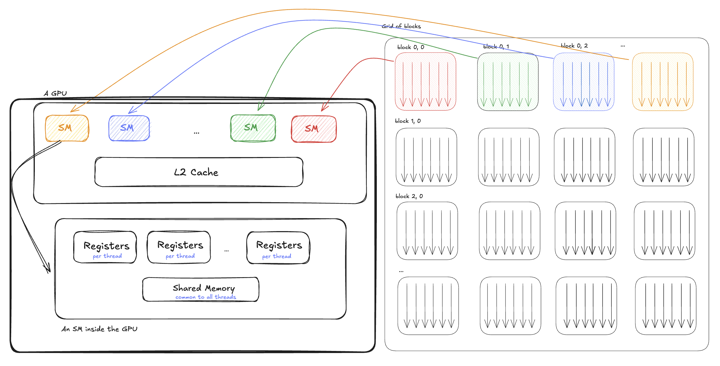
So to recap, we mentioned that we launch a grid of CTAs—each CTA contains a contiguous array of threads—and each CTA is scheduled on one SM.
If we dig deeper into the execution model of a CTA, we note that each block is further subdivided into a set of warps. A warp consists of 32 threads that run the program counter in lockstep. So if we launch a block of 128 threads, we would implicitly have launched a block of 4 warps. The two are synonymous, and no additional programming on your part is needed.
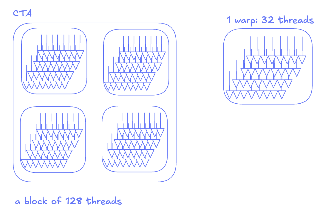
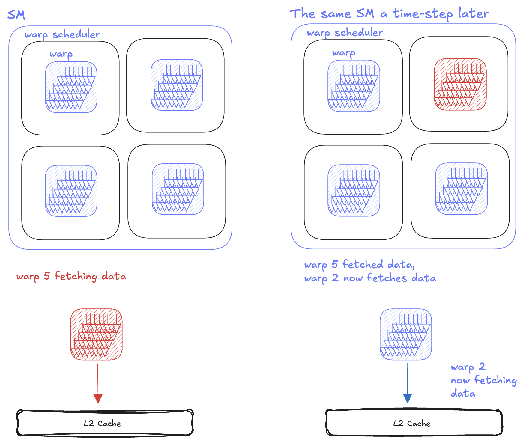
Each SM internally has 4 warp schedulers (physical units that issue instructions by the granularity of a warp). Different warps can execute in parallel on different warp schedulers and concurrently on the same warp scheduler.
This is useful because an SM can yield to other warps if the instructions are not ready to be executed on the current warp—thus giving the programmer some latency hiding. For example, if a warp requires data from memory, it has to wait till that data is fetched. Instead of sitting idle, the warp scheduler swaps it out for another warp that has its data ready. That way, the GPU is never idle.
This programming paradigm is not exclusive to Blackwell, the grouping of threads into warps has been the case for virtually the past 2 decades – since NVIDIA’s Tesla architecture.
Thread block clustering
On Hopper and Blackwell, programmers can group multiple CTAs into a cluster. A cluster guarantees that its blocks are scheduled on SMs that are physically connected within the same GPU Processing Cluster (GPC). This proximity allows blocks on different SMs within the cluster to directly access each other’s shared memory, bypassing global memory and effectively enlarging the available shared memory space. As a result, the GPU execution hierarchy now includes an additional layer: the cluster, positioned between the block and the grid.
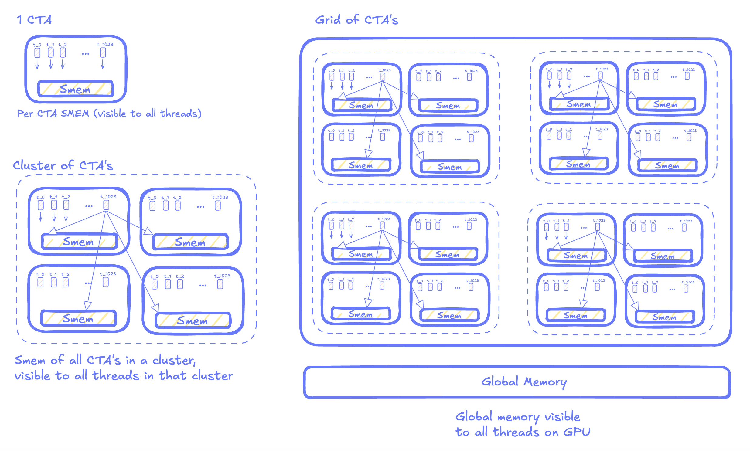
Visualized, this how a cluster will get scheduled on the GPU:
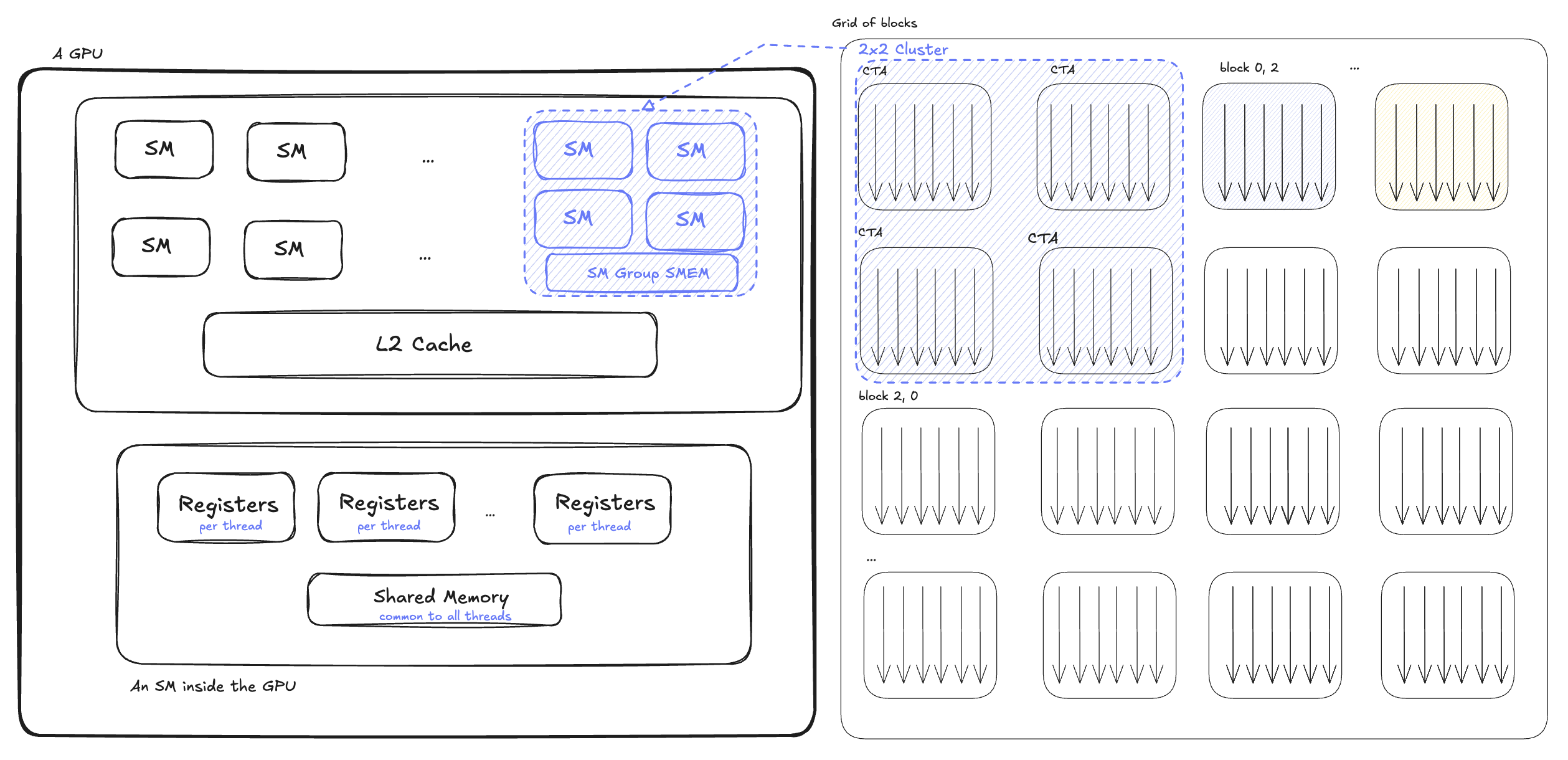
Now that we’ve explained the entire GPU programming paradigm, we can almost write our first kernel. However, before we do so, let’s take a trip down memory lane and look at the evolution of the GPU hardware, and what features the hardware provides to enable us to squeeze the best performance out of each GPU.
NVIDIA’s GPUs - A look over the past 3 generations
NVIDIA has transformed GPU architecture over the past five years through a series of groundbreaking platform releases. From the Ampere architecture's introduction in 2020 to the cutting-edge Blackwell platform, each generation has delivered substantial gains in computational performance, memory bandwidth, and AI acceleration capabilities. This section examines the defining features and innovations of the Ampere, Hopper, and Blackwell architectures.
NVIDIA's Ampere architecture
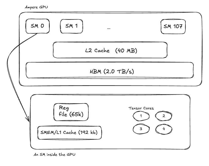
Released in May 2020, Ampere advanced Tensor Cores considerably (even though tensor cores were introduced a few generations earlier) From a spec point of view, Ampere had:
- 108 Streaming Multiprocessors (SMs)
- 4 Tensor Cores per SM
- 80GB High Bandwidth Memory (up to 2.0 TB/s)
- 192KB combined Shared Memory + L1 cache per SM
- 65,536 registers per SM
- 40MB L2 Cache shared between all SMs
- Asynchronous copies to allow deeper software pipeline between global -> shared memory copies
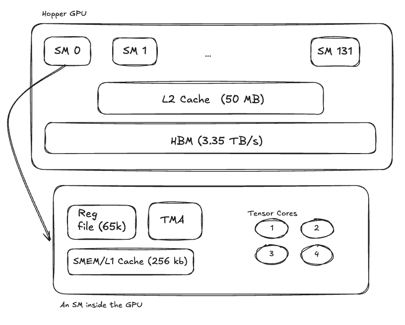
NVIDIA's Hopper architecture
Released in late 2022, Hopper improved upon Ampere, and is still considered for wide LLM deployments today. Hopper had the following specifications:
- 132 Streaming Multiprocessors (SMs)
- 4 Tensor Cores per SM
- 80GB High Bandwidth Memory (3.35TB/s)
- 256KB combined Shared Memory + L1 cache per SM
- 65,536 registers per SM
- 50MB L2 Cache shared between all SMs
- Introduced a TMA engine to optimize block memory copies
- Is not forward compatible with next generation hardware
NVIDIA's Blackwell architecture
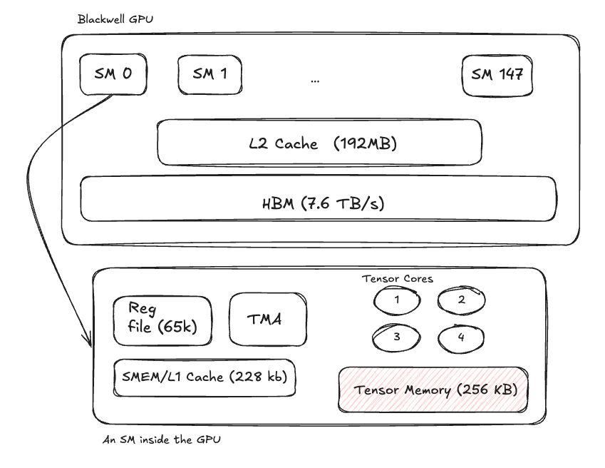
Blackwell is the latest NVIDIA architecture and is currently the SOTA architecture for LLM deployment. It improved upon Hopper and Ampere by increasing the compute capacity as well as providing a few key features to enable faster execution:
- 148 Streaming Multiprocessors (SMs)
- 4 Tensor Cores per SM
- 7.672 TB/s High Bandwidth Memory
- 228 KB combined Shared Memory + L1 cache per SM
- 65,536 registers per SM
- 192 MB L2 Cache shared between all SMs
- 5th Generation Tensor core architecture
- 256 KB of Tensor Memory
Blackwell’s architecture can be more or less visualized as follows:
GPU comparison at a glance
To give the reader’s a sense of the magnitude of the differences, here’s a table comparing peer-to-peer performance:
| Metric | A100 (Baseline) | H100 | H200 | B100 | B200 |
|---|---|---|---|---|---|
| Peak Memory Bandwidth | 1.0x | 1.6x | 2.4x | 3.9x | 3.9x |
| NVLink Bandwidth | 1.0x | 1.5x | 1.5x | 3.0x | 3.0x |
| Peak BF16 TFLOPS (dense) | 1.0x | 3.2x | 3.2x | 5.6x | 7.2x |
| Peak FP8 TFLOPS (dense) | N/A | 1.0x | 1.0x | 1.8x | 2.3x |
As the GPU becomes more powerful in terms of FLOPs/s and bandwidth, the programming model to achieve this peak performance also evolves. Below is a review of the optimal operation scheduling on different architectures.
Pre-Ampere optimization
Ampere introduced asynchronous data movement. Before Ampere, memory operations blocked compute, and we had to do something like: Load data from global → Wait → Compute → Wait → Store results
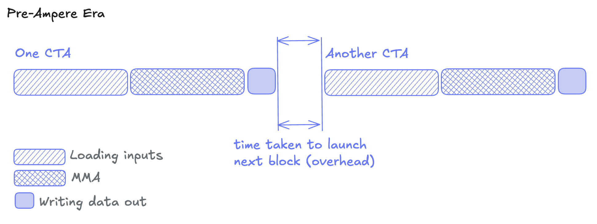
As a result, one would perform double buffering operations on pre-Ampere architecture and use multiple CTAs per SM for overlapping data transfer and computation. This caused contention for the SM’s limited memory resources, and force trade-offs between memory latency and optimal tiling.
Ampere optimization
With Ampere's async copy instructions (cp.async), one can pipeline the data loading and MMA operations and achieve overlap within a single CTA.
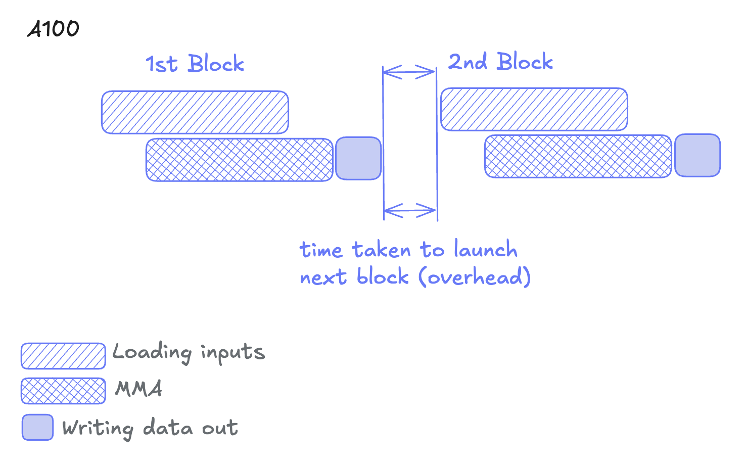
Using the cp.async instruction, threads can issue memory copies and immediately move on to next work, hiding memory transfer latency behind mma operations.
✅ Ampere’s win: Overlapping input loads with computation
❌ Ampere’s problem: CTA launch overhead
Hopper optimization
Hopper architecture introduces new instructions for data transfer and mma:
- TMA (Tensor Memory Accelerator): TMA is a dedicated hardware unit for moving multi-dimensional tensors. Instead of each thread calculating addresses and loading individual elements, TMA transfers a tensor tile asynchronously between global and shared memory.
- Asynchronous Warpgroup MMA (WGMMA): While Ampere enables overlapping MMA (synchronous instructions) with data transfer, the WGMMA instructions are asynchronous and allow overlapping of the mma with not only the memory access, but also core computations.
As a result of this, a new paradigm of matmul development arose which is called Persistent Kernels. This technique will be discussed in depth in subsequent blog posts, but at a high level, it allows CTAs to stay resident on an SM and process multiple tiles without returning to the host. This eliminates kernel launch overhead and overlaps one work tile's output with next tile's loading.
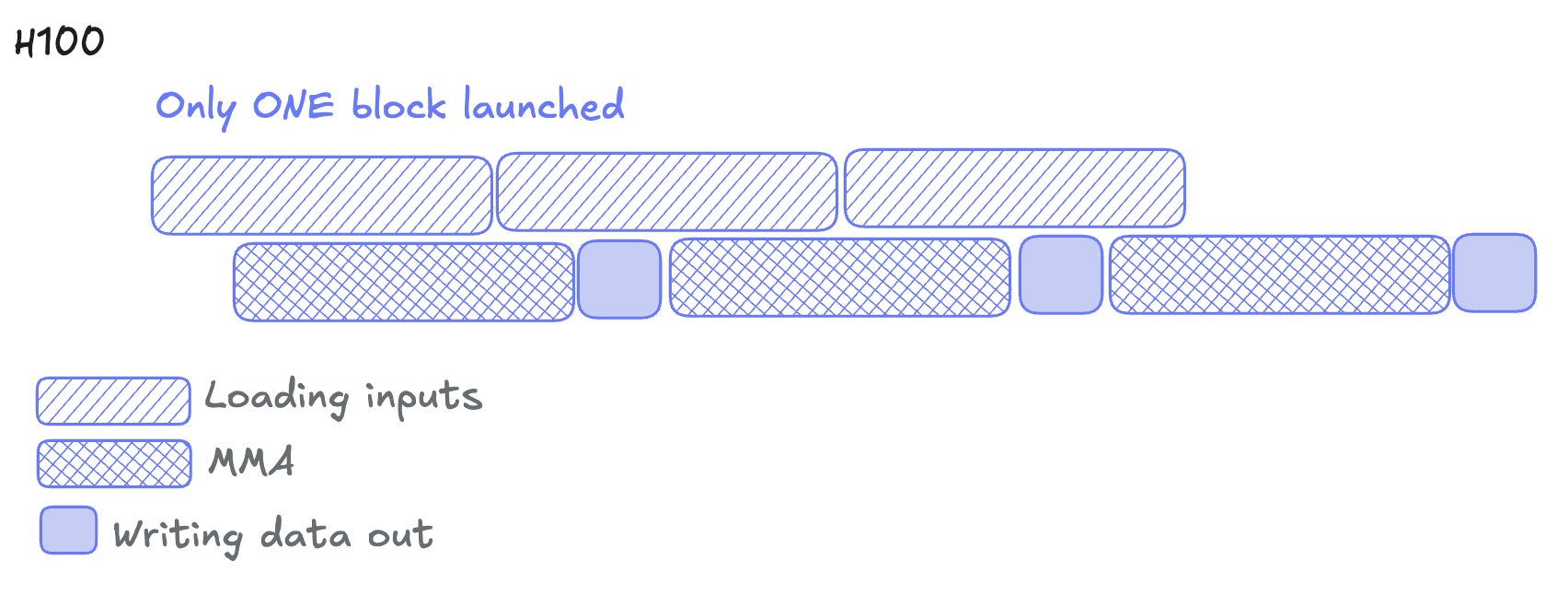
✅ Hopper’s win: Reducing CTA launch overhead and overlap data transfer across tiles.
❌ Hopper’s problem: WGMMA consumers use lots of registers and contention between the tensor core and the ALUs.
Blackwell optimization
Blackwell architecture introduces tcgen05 instructions and tensor memory, where the MMA's result is stored on new, dedicated hardware- tensor memory. This breaks the WGMMA’s dependency on registers. We can now leverage even more pipelining without polluting those registers.
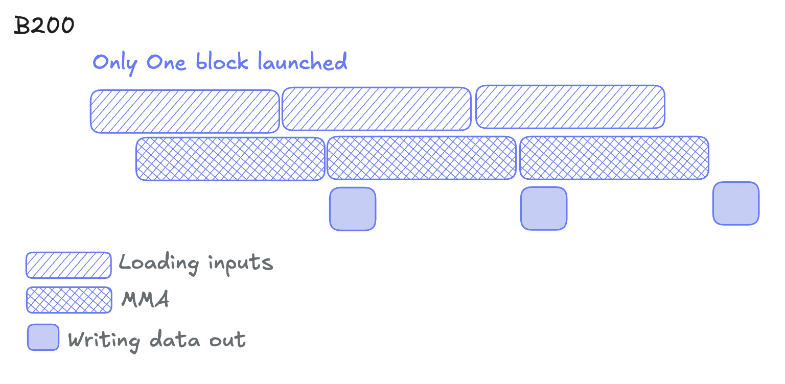
This creates a three-stage pipeline:
- Loading inputs (TMA) - load the data via the TMA engine
- Computing MMA (Tensor Cores) - compute the MMA operations and write into tensor memory
- Storing outputs (from Tensor Memory) - store the results from tensor memory into global memory
All three stages can run concurrently on different memory regions. Thus tile N computes, tile N+1 loads, and tile N-1 writes out—forming a software pipeline.
✅ Blackwell’s win: pipelining the write-out stage
❌ Blackwell’s problem: Tensor memory only supports very limited instructions
As shown, the algorithm for achieving peak performance becomes more sophisticated as the hardware advances. In fact, the CUDA programming model also falls short- lots of the instructions, like tcgen05, are only available in PTX. This is not ideal, and is where Mojo steps in to fill the gap.
Matmul in four lines
Armed with the understanding of GPU programming and the hardware, we can now, finally, translate our matmul function over to a GPU matmul kernel. This is trivial, and can be done like so:
We created a 2D grid of threads large enough to cover our entire C matrix:
- Each thread computes one element of the output matrix
C, and that element is based on that thread’s unique id row = global_idx.y
col = global_idx.x- Thread blocks are mapped to tiles of the output matrix
The kernel does this dot product for every output in the C matrix, all at once.
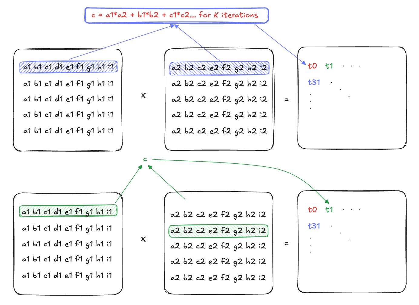
The inputs to the matmul function is a LayoutTensor. To learn more about LayoutTensor, see Using LayoutTensor in the Mojo Manual
This allows us to abstract away the algebra required to index/offset into memory to fetch it (for instance, for matrix A, that would’ve been a[row * K + col] ).
Data types and casting
Since we are interested in LLMs, and since BFloat16 is the most popular data type in LLMs, we will be using BFloat16 throughout this series. This is a half float data type which is stored in 2 bytes of memory, and is similar to the Float16 data type but comes with additional benefits:
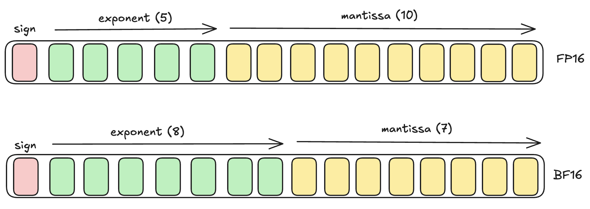
Since the exponent range in BF16 can vary from -126→127, it can represent a much larger range of numbers from the traditional FP16. Its maximum positive value is: $$3.39x10^{38}$$ compared to that of FP16, which is: $$6.55x10^4$$ This larger range makes it great for deep learning applications and LLMs, where you need to accommodate gradients over many orders of magnitude, and where precision of individual values is not critical.
There is however a catch: when accumulating many values (K iterations), rounding errors in BF16 compound rapidly (because its Mantissa is small, it has a smaller granularity between hops). To prevent this, we can change our code to accumulate the intermediates in higher precision:
Using FP32 for accumulation preserves numerical accuracy during the reduction, while still getting the memory benefits of BFloat16. Note that tensor cores would accumulate BFloat16 in Float32 as well. The reduction result is then downcast to BFloat16 before storing to global memory.
To measure the performance of our kernel, we run the code and measure how many FLOPS (FLoating-point OPerations per Second) it achieves. In this setup, we multiply matrix A(MK)*B(KN) = C(MN). There are MN elements in the output, each of which took a dot product of size K (K multiplications and K additions). Hence, our kernel does (MN)2K flops in total, and the performance, in FLOPS, is calculated as 2MNK/time. Our kernel gives us 5 TFLOPs.
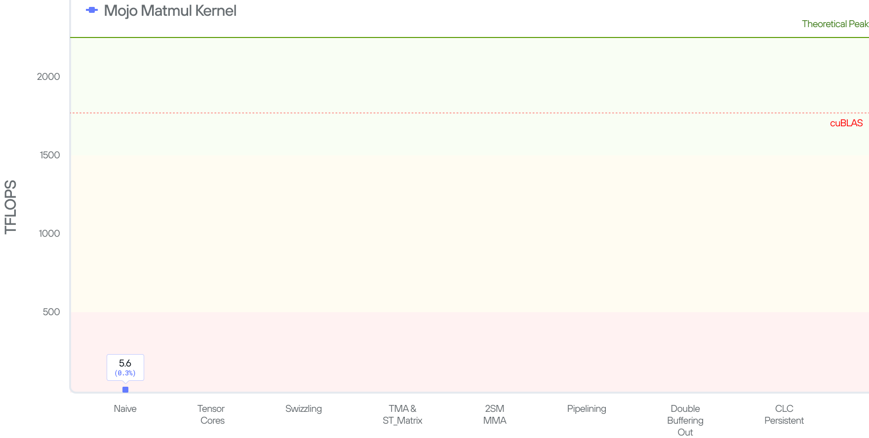
The 5 TFLOPs is not bad (given that the code is only 4 lines), but is also not great considering cuBLAS’ SOTA 1763 TFLOPs and a peak theoretical performance of 2250 TFLOPs on the B200 system.
In the next set of blog posts we will show how we gradually bridge that gap by leveraging the Tensor cores and the other Blackwell features that we have discussed.
Read all 4 parts of the "Matrix Multiplication on Blackwell" Series:
Part 1 - Introduction
Part 2 - Using Hardware Features to Optimize Matmul
Discover what Modular can do for you


