


🛠️ Code to all kernels mentioned in this series is available on GitHub.
In this post we are going to continue our journey and improve our performance by more than 50x our initial kernel benchmark. Along the way we are going to explain more GPU programming concepts and leverage novel Blackwell features. Note that this is not the end of the blog series, and we will continue to improve upon the methods presented here in subsequent blog posts.
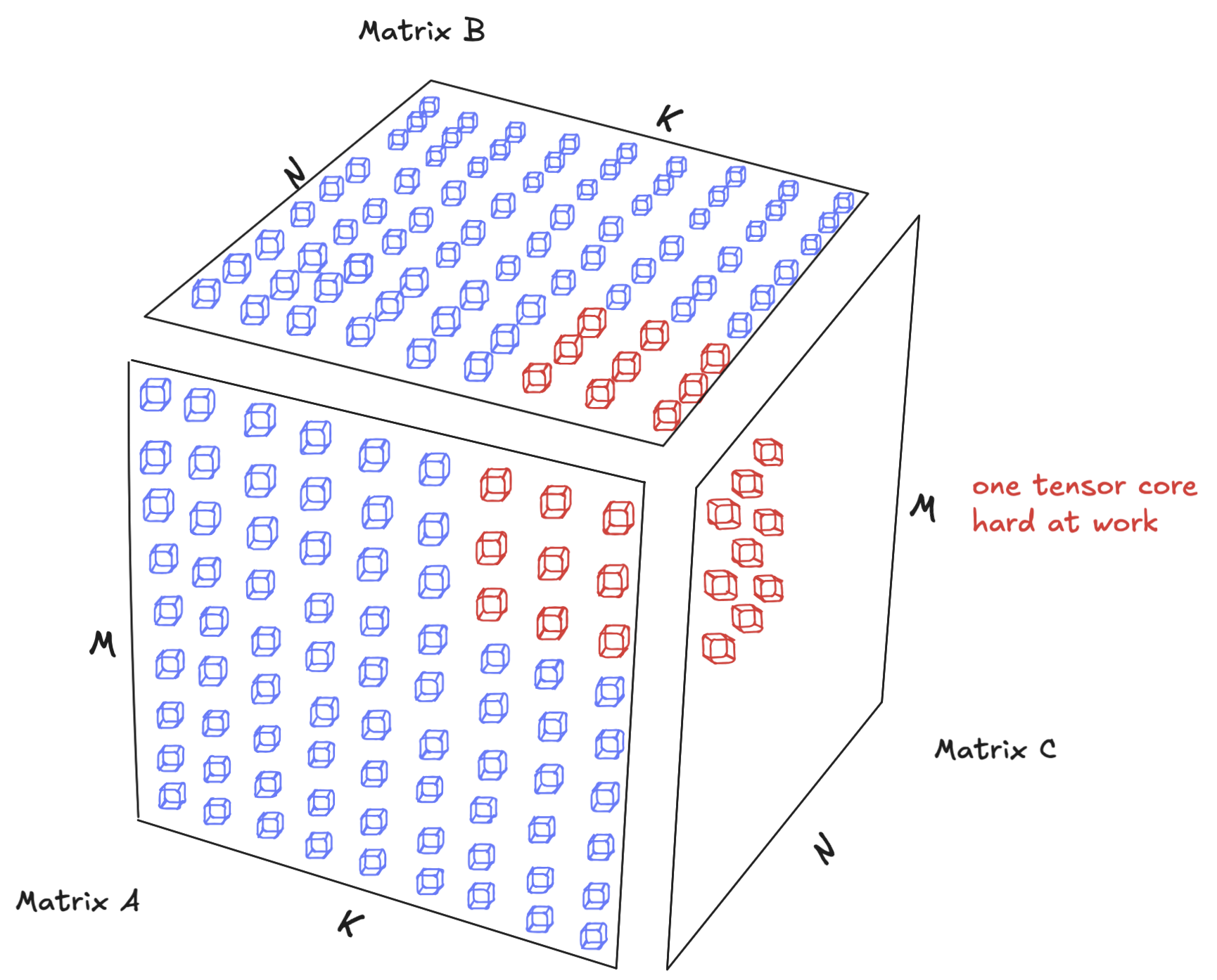
To keep things simple, we will be looking at a specific shape of matmul where the A matrix is MxK, the B matrix is KxN (transposed), and the resultant C matrix is MxN with M=N=K=4096. We’ll assume the same shape throughout this blog series; in the last post we’ll show how our techniques generalize to any shape.
Recall our 4 line matmul from before, and let’s zoom in on the core computation:
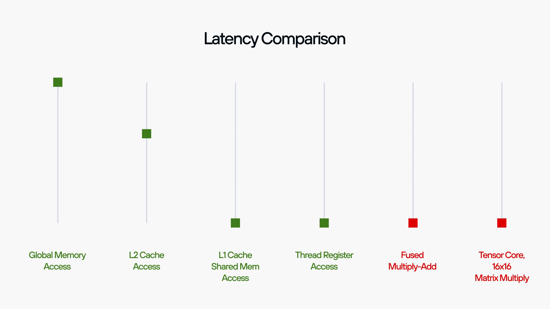
Each Fused Multiply Add (FMA) operation requires two global loads and one memory write. The issue with global memory is that, while abundant, it's considerably slower than other kinds of memory. Therefore the craft of optimizing matmul is how to avoid or hide the memory loads and stores by leveraging the memory hierarchy available on the GPU. The following figure visually explains the latencies of different operations we will be using over the course of this series.
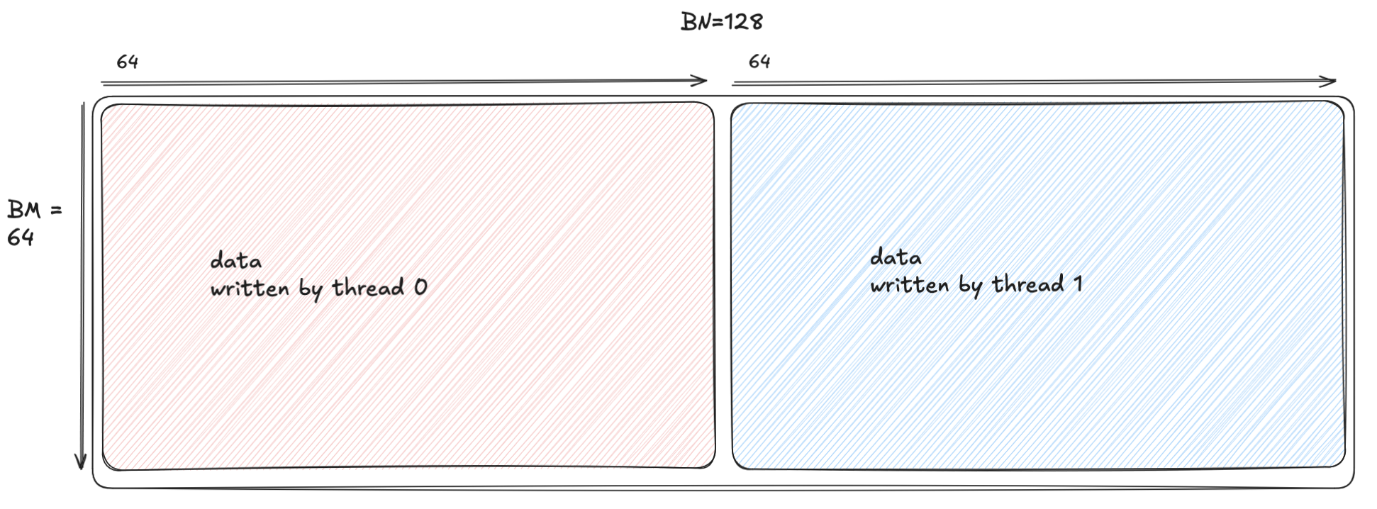
Taking a step back, we can visualize the memory access for our 4-line matmul by assigning a different color to each thread, then illustrate how each thread reads data from the input matrices.
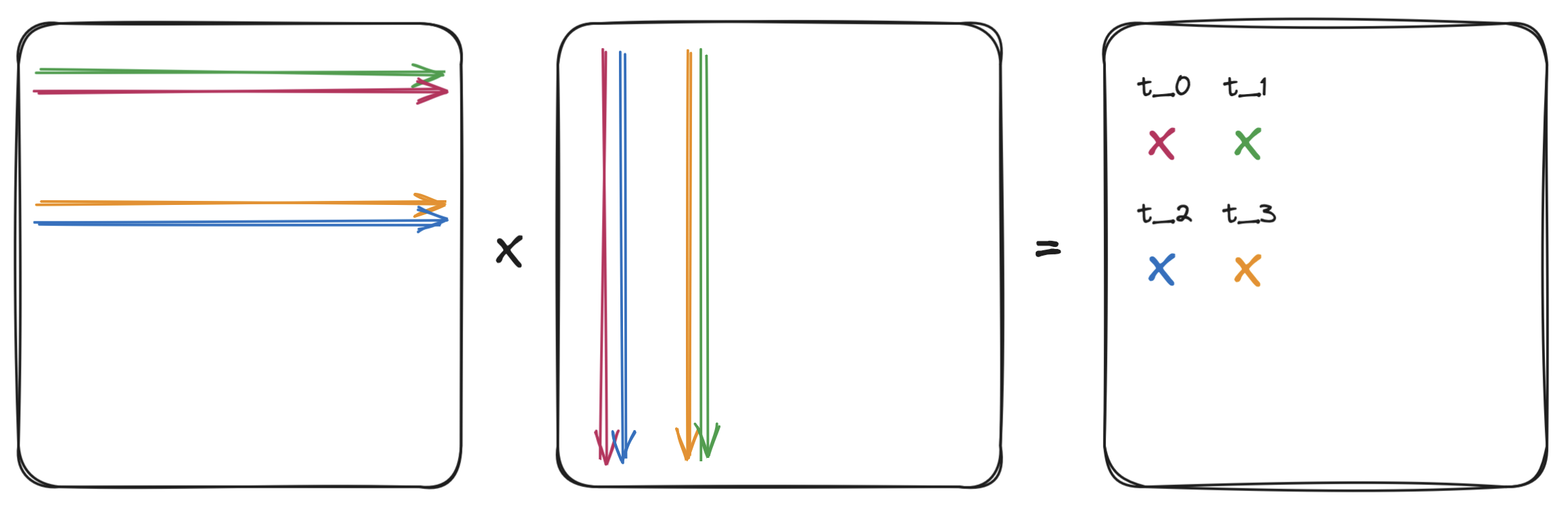
- Thread 0 computes C[0, 0], reads row 0 in A and column 0 in B
- Thread 1 computes C[0, 1], reads row 0 in A and column 1 in B
- Thread 2 computes C[1, 0], reads row 1 in A and column 0 in B
- Thread 3 computes C[1, 1], reads row 1 in A and column 1 in B
Considering just four threads, note that each thread loads one complete row and one complete column to calculate a single output value. If we count the number of memory loads for all fours threads, the load for each row and column is repeated twice. These observations point us towards the first improvements that we can make: reducing slow global memory access.
Shared memory
A common technique to reduce redundant loads is called loop tiling. The idea of tiling is simple. One loads small tile of the matrix into a much faster memory cache, so the processor can perform all the necessary calculations on that block of data without constantly having to go back to the slow main memory. Once it's finished with one tile, it loads the next one.
We'll use shared memory as a cache, and since each Blackwell SM gives us 228KB of shared memory, it means that we could share data between multiple threads and perform tiling across a block. Here’s what we’ll do:
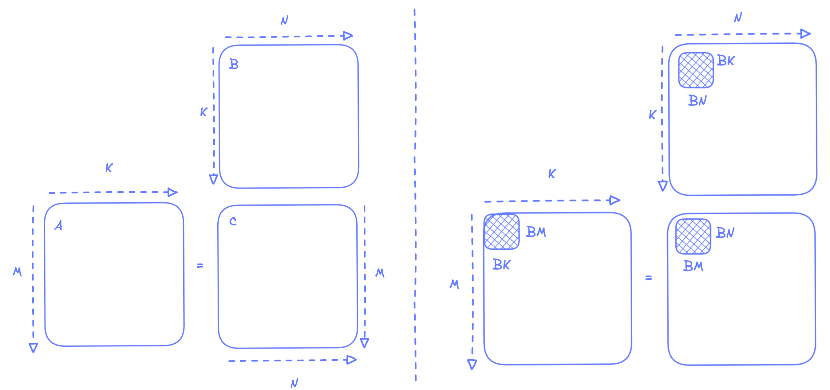
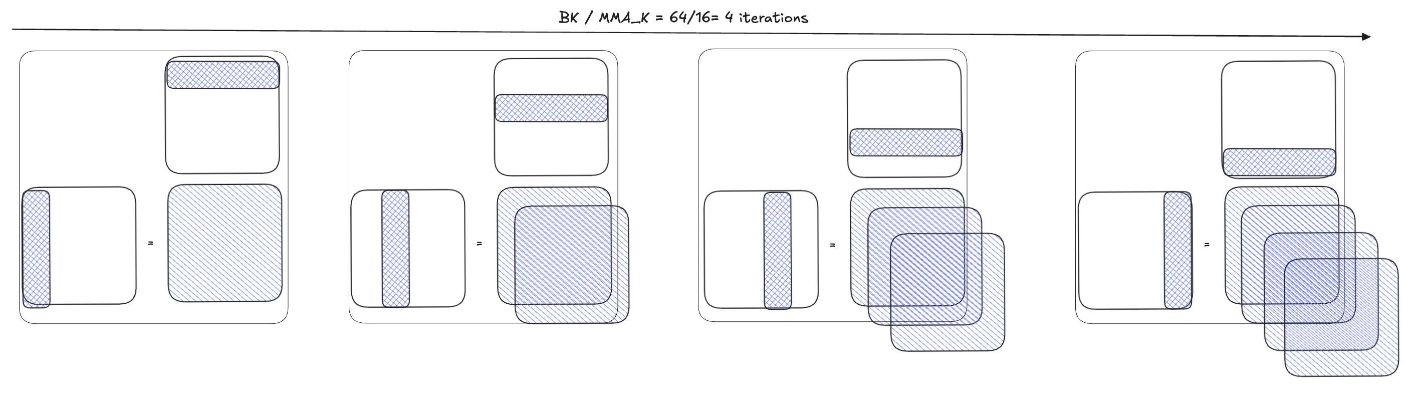
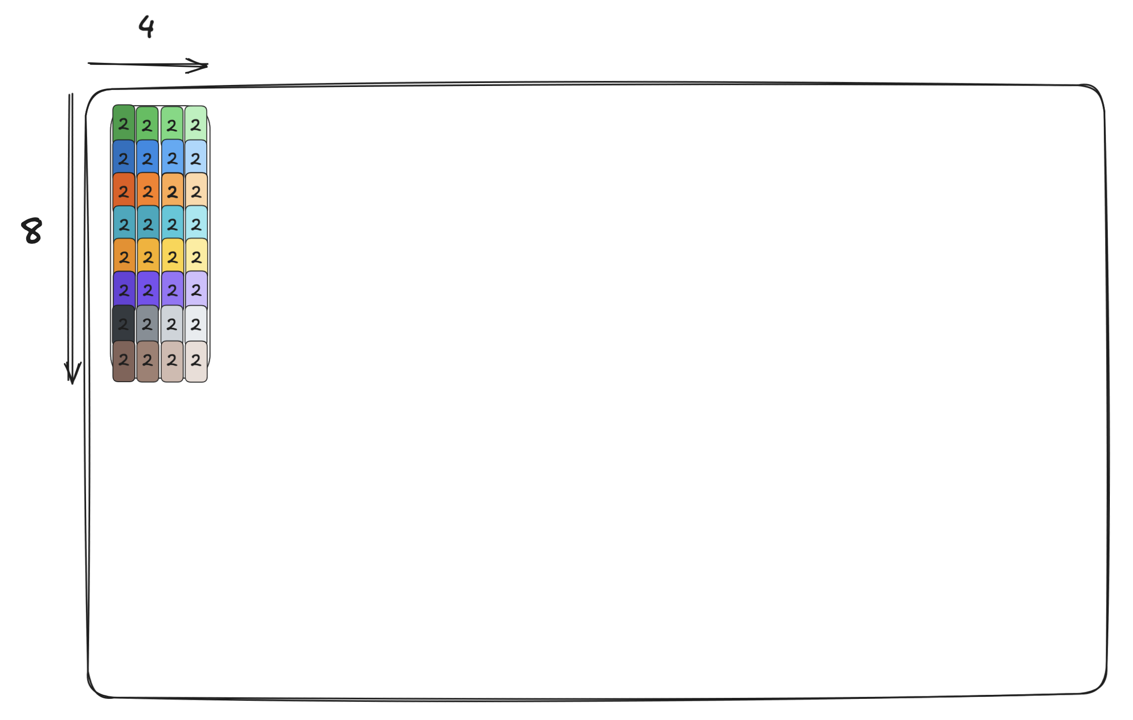
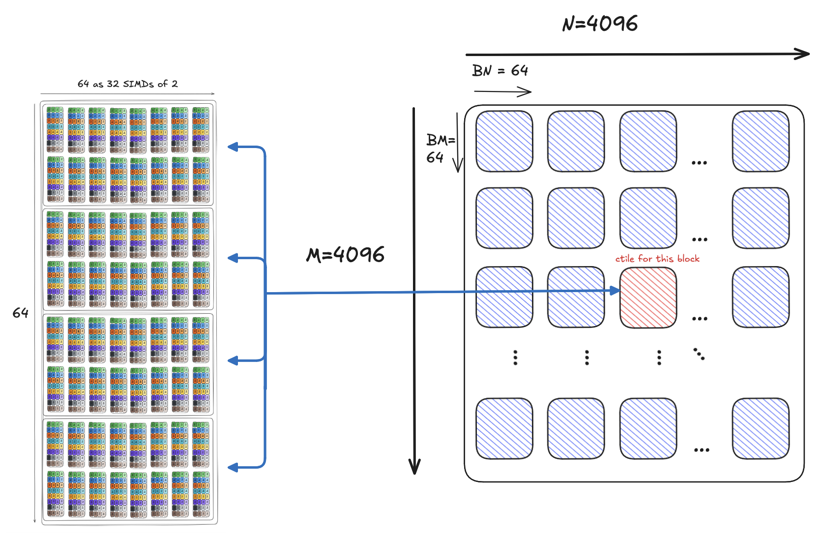
We will partition our matrix into tiles, BMxBK tiles for matrix A, and BNxBK tiles for matrix B, where BMxBNxBK=64x64x64 . We will discuss the possible numbers and the restrictions later, but for now, these can be treated as tiles for our 4096x4096 square matrices. The only constraint that we should be aware of right now is that the tile doesn’t exceed the size of shared memory.
For the first iteration within a K/BK loop, we load a tile of size BMxBK from matrix A and BNxBK from matrix B. We know this can fit into our shared memory, since that’s two 64x64 tiles, or 8192 2-byte elements. This results in a memory requirement of about 16KB for each block, which is far less than the 228KB of available shared memory. We then perform the matrix-multiply-accumulate (MMA) operation on this tile, and store the result as an intermediate value:
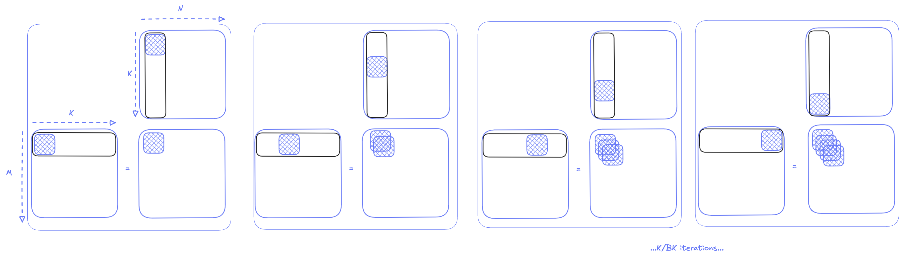
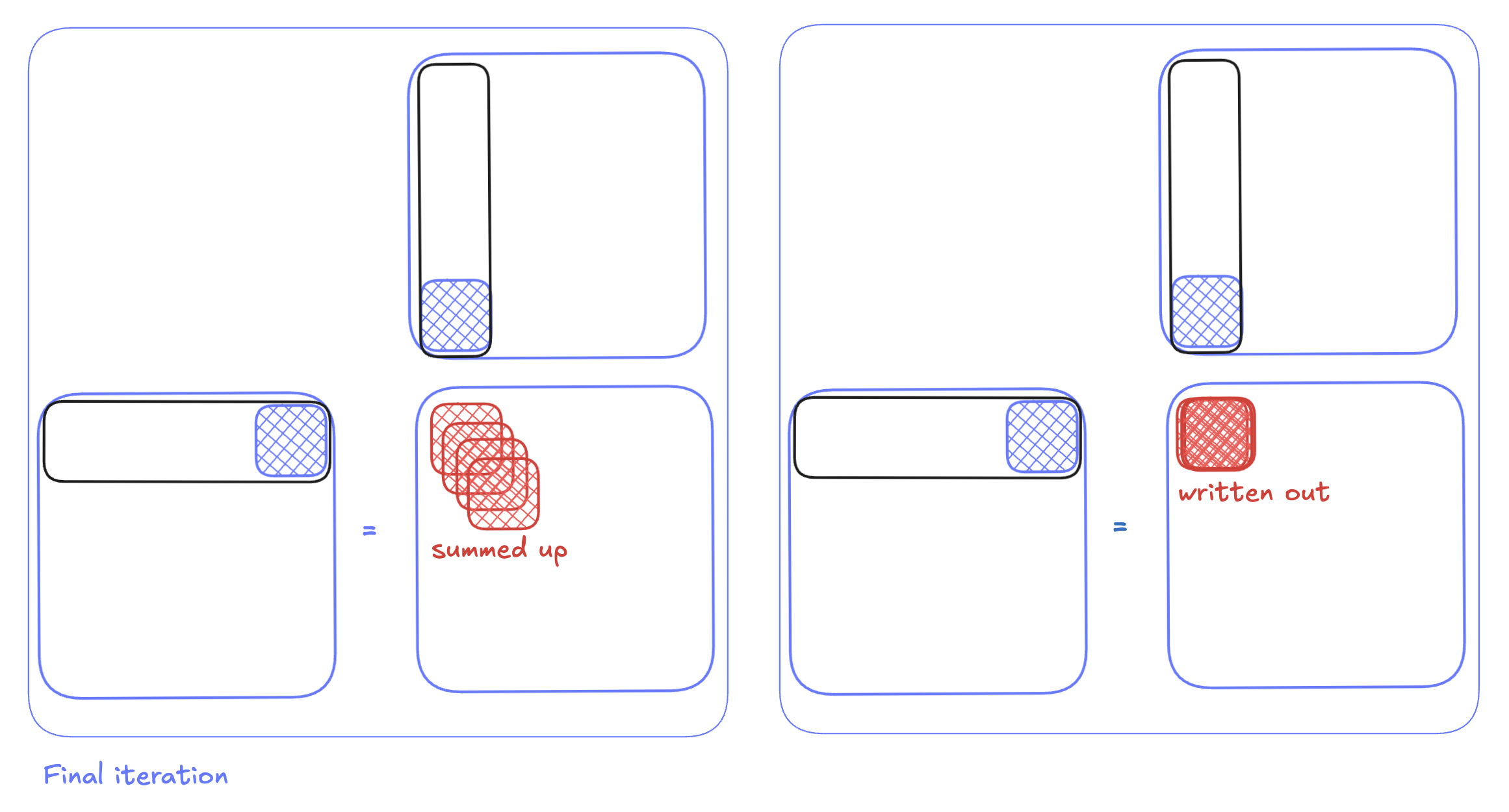
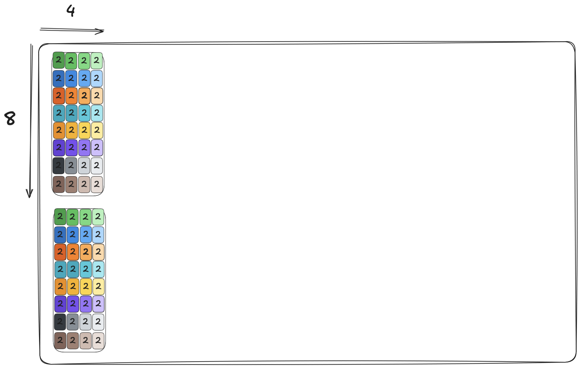
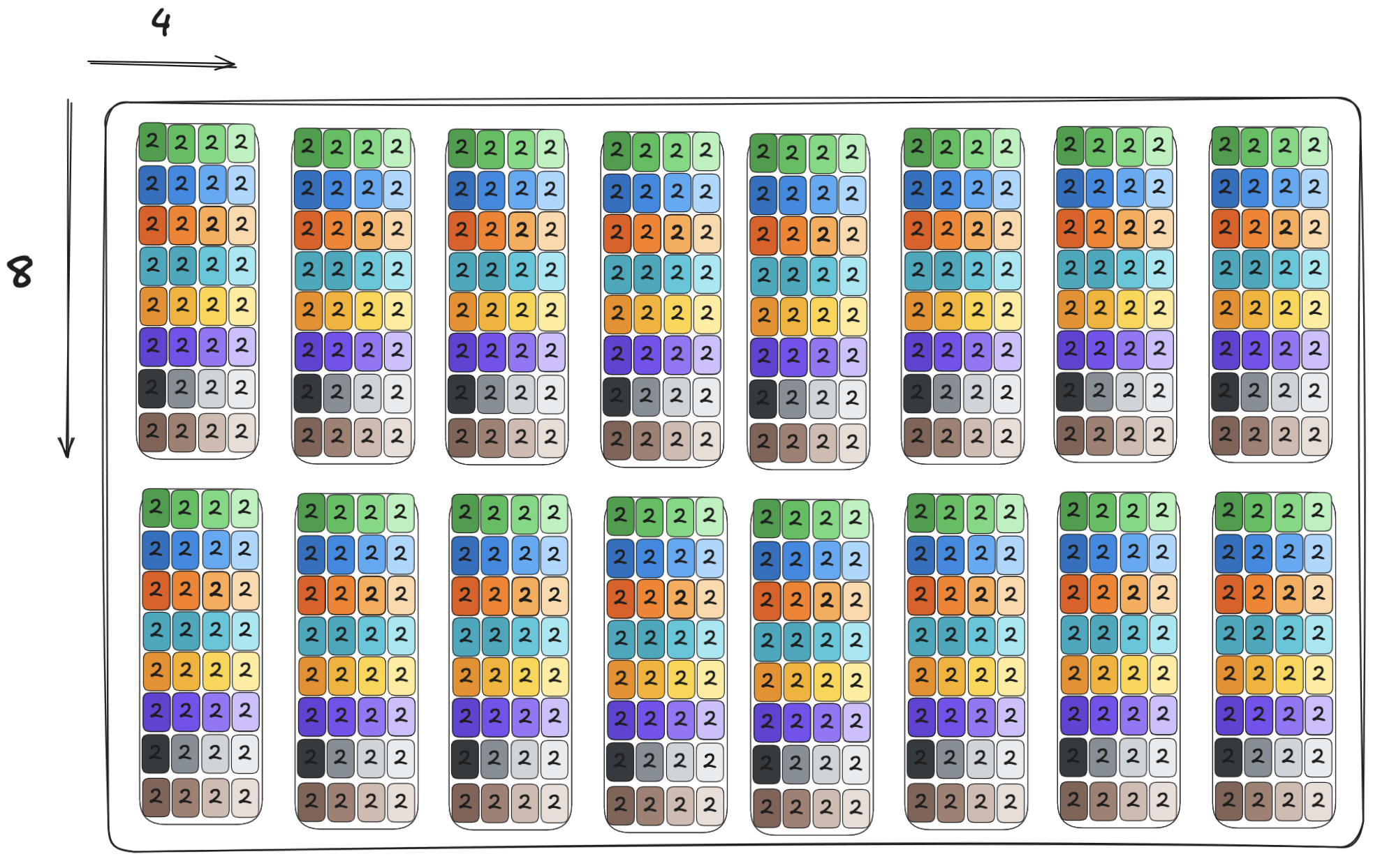
In the second iteration, we load the next two chunks into shared memory, and we add the result of this MMA to the result from the previous iteration.This keeps going on for K/BK iterations (in our case 256 iterations) until we reach the result of the final tile. Once the K/BK loop in done, we will have the final output tile. The final result for that tile can then be written only once to global memory.
With this idea sketched out, we can now move on to our second, improved matmul kernel implementation.
Kernel 2: TMA and tensor cores
In this section we will develop our next kernel. Kernel 2 is more advanced that the initial kernel and will use both tiling and tensor cores for optimization. Follow along with the code here. As a rough idea, here is what the kernel will do:
We will store our B matrix in its transposed form to ensure coalesced layout when accessing. This can be done via a Layout transform:
The kernel does require some host setup changes, and we will explain the needed changes on the host incrementally.
1 - Loading tiles into shared memory
The NVIDIA Hopper architecture introduced the Tensor Memory Accelerator (TMA), a specialized hardware unit that transfers data between the GPU’s global memory (GMEM) and shared memory (SMEM) asynchronously.
To use the TMA, we need to first create a tensor tile on the host and pass it to the kernel. The tensor map is a 128B data chunk encoding the input tensor's shape, the stride, and the global memory address. (The tensor map can also encode a swizzling pattern, an optimization we’ll discuss a little later.) You can easily create a TMA tile in Mojo using the provided APIs:
Below is how we use the TMA object within the kernel:
At a high level, one thread (elect_one_thread) launches the asynchronous copies and use a memory barrier (tma_mbar) to guard that the copies are completed. Let’s go through this one at a time.
a_tma_op.async_copy takes three arguments:
a_smem_tile:aLayoutTensorproviding the tile’s shared memory addresstma_mbar:a memory barrier to track how much data has been transferred(i * BK, block_idx.y * BM):is the current tile’s coordinates in global memory, depending on the iteration and block coordinate (see part 1)
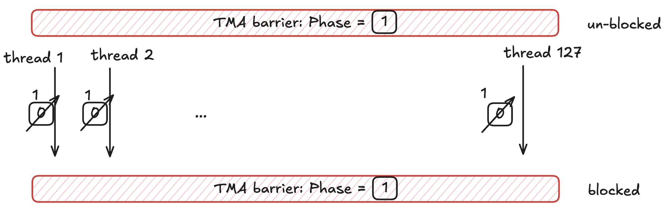
The need for a TMA barrier
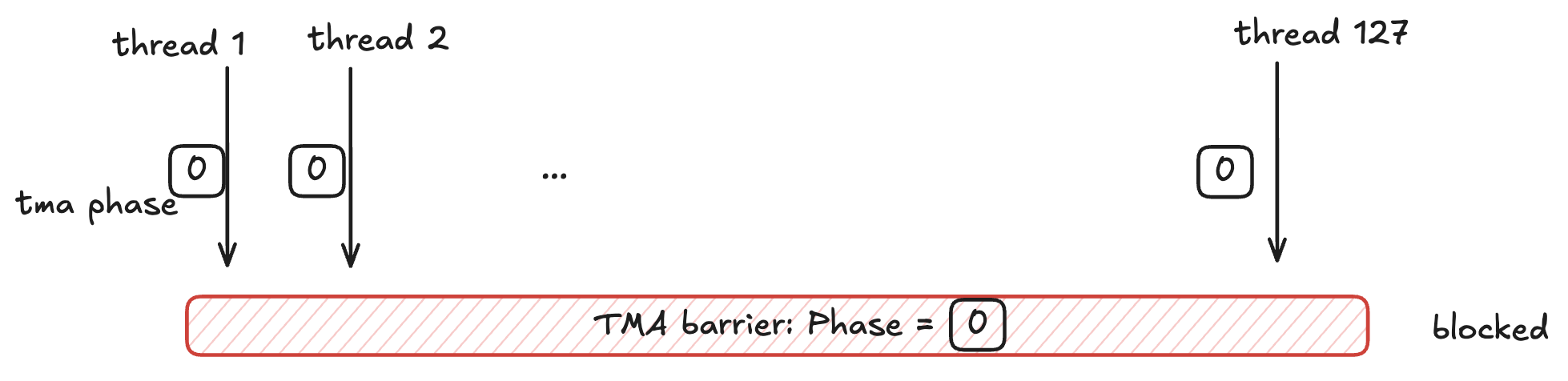
Because the TMA operation is async, we need to implement some way to ensure the MMA cannot proceed until the tiles are fully resident in shared memory. This is why we use a memory barrier (mbar), such that the threads will wait/block on this barrier until the tiles are copied to shared memory.
This is done by initializing each thread with its own barrier phase (tma_phase=0). The memory barriers have their internal phase value initialized also to 0. When the phase of a thread matches the phase of the barrier, the thread can not unlock the barrier, and it can not pass. Only when the two phases differ can the thread proceed.
The above code causes the threads to block and if we trace the execution it would look like:
Prior to the TMA transfer, the barrier is initialized with how many bytes to expect from the TMA with tma_mbar[0].expect_bytes(expected_bytes). The expected bytes is the total number of bytes in both transferred tiles.
The TMA continuously updates the barrier with the number of bytes it has transferred, and once the number of bytes transferred reaches that of the total bytes, the phase of the barrier flips and the threads can proceed.
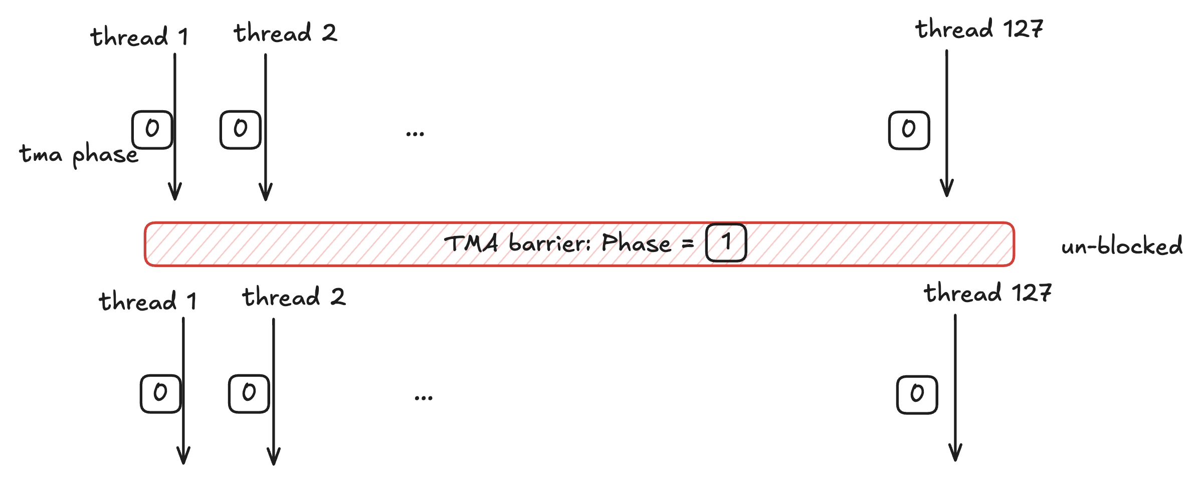
We then manually toggle the tma_phase of each thread via tma_phase ^= 1 to ensure that the threads block on the next iteration until the TMA transfers that iteration's tile into shared memory.
Mojo does provide abstractions that hide some more TMA details and optimization tricks for you. For example, if we ask you what the a_tma_op layout is, what would your answer be?
💭 We said the tile isBM x BK, so ifBMis64andBKis64, then the((shape), (stride))tuple is((64, 64):(64, 1)), given that it isRow-Major/K-Major.
And you would, of course, be correct! Then if the question is so how many fetches will the TMA unit need to load our 64x64 tile?
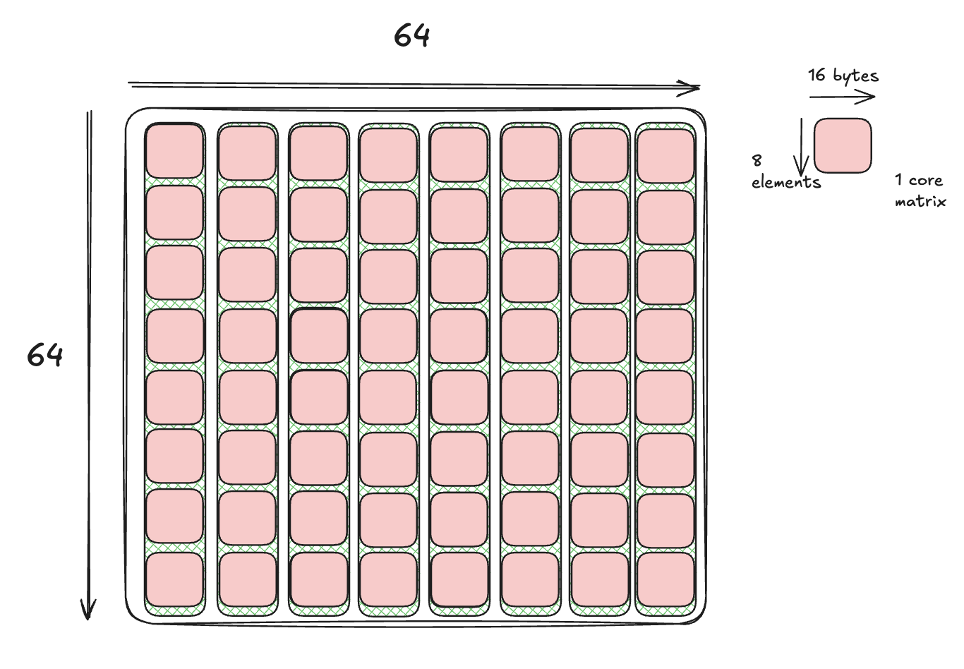
💭 Well, since it’s declared with a 64x64 layout, obviously one.And you would, of course, be wrong. It actually takes 8 fetches to load the tile. While we specify a logical tile size of 64x64, the TMA hardware partitions our 64x64 tile into eight 64x8 sub-tiles, and loads them one at a time. To explain why we have to do it this way, we need to introduce "core matrix."
Core matrices
There is a hidden nuance with TMA, Tensor Cores, and NVIDIA GPUs at large: the core matrix.
The concept is simple. tensor cores don’t understand elements, they understand matrices. They can only view the matrix as a group of 8x16B tiles—that’s core matrices of 8x8 elements as far as we’re concerned.
tcgen05.mma supports 8 canonical layouts of core matrices in shared memory (inherited from WGMMA) based on the layout (row-major or column-major) and swizzling mode. Our current kernel uses K-major for both A and B, corresponding to a layout where each column of core matrices (8x1) needs to be contiguous in shared memory. This is why the descriptor layout shows (64, 8)—the TMA copies one column of 8 core matrices at a time, and this operation will be repeated 8 times to fill the 64-element width of the tile.
Of course, our Mojo library’s async_copy abstracts this complexity away from you, such that a programmer only has to issue a copy, and can expect the tile to show up in shared memory.
2 - Issuing the MMA instructions
To recap a bit, the 5th generation tensor cores introduced in Blackwell come with a new set of instructions (tcgen05 instructions) and 3 fundamental improvements for the MMA operation:
- Increasing the largest
tcgen05.mmashape to128×256×16for a single SM, compared to the previous64x256x16on Hopper. This means we almost double the throughput. - Introduced 2SM
tcgen05.mmawith up to256x256x16(we will explain the 2SM operation in a subsequent blog post in this series). - Decreased register pressure by introducing a new kind of memory called Tensor Memory. This allows the
tcgen05.mmainstruction to store its result in Tensor Memory instead of register memory. But what is tensor memory?
What is Tensor Memory?
There is another improvement in Blackwell which we mentioned briefly in the first part of this blog series, and that is Tensor Memory (TMEM).
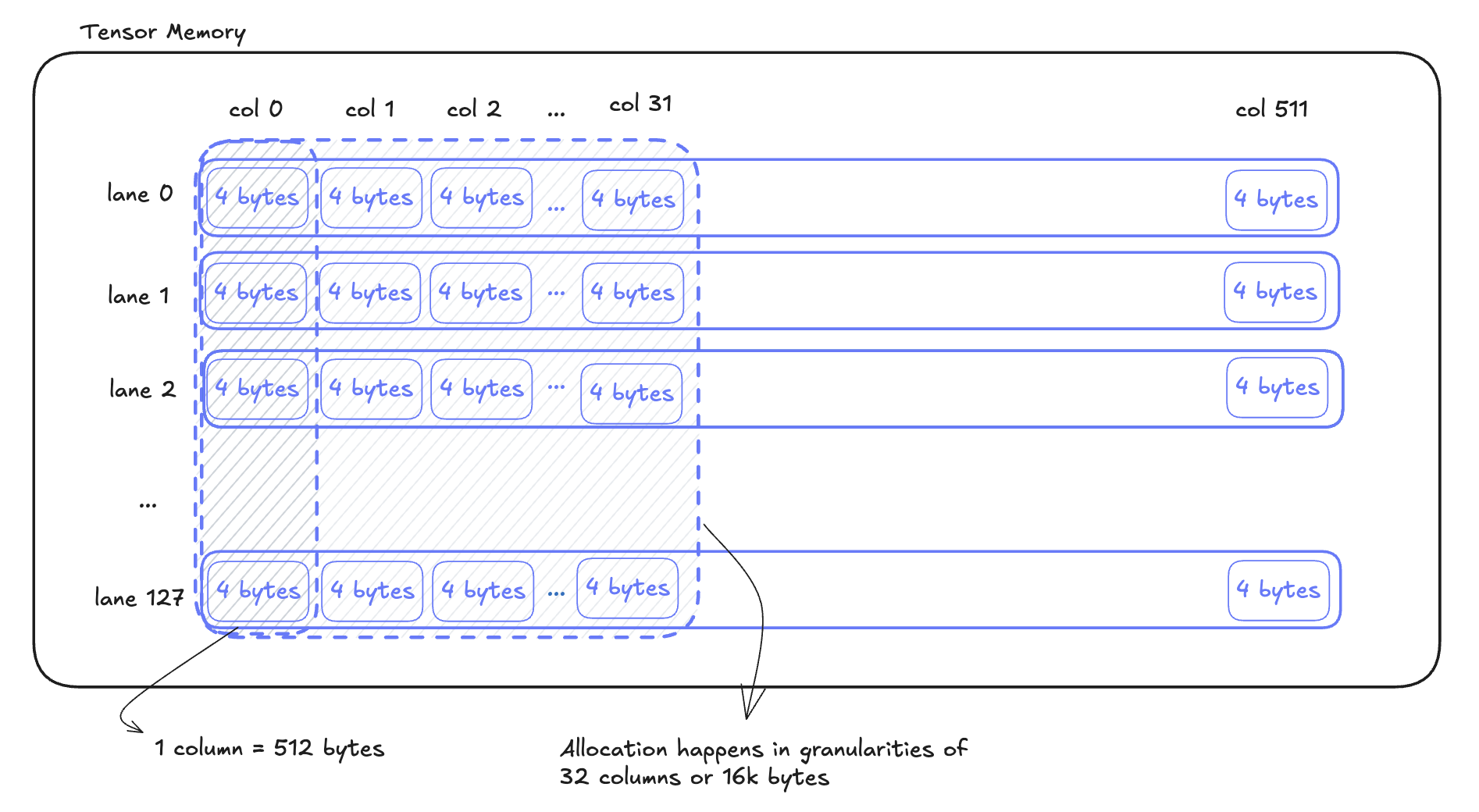
TMEM is a 256K on-chip memory space specialized to store the input or output for tcgen05 MMA instructions. There are 128 lanes of 512 columns, for a total of 65,536 elements. Each element is 4 bytes, for a total of 256KB. Allocation is done by columns, and the granularity of allocation is 32 columns, meaning the smallest you can allocate is 32 columns (16k bytes) at a time.
Prior NVIDIA generations would have had to use general purpose registers to store matmul results which has a few issues:
- Register space is scarce, with only 64k registers per SM. Thus there was a contention between the Tensor Cores and the general purpose ALUs.
- Registers are thread-private while MMAs were wrap-level operations in pre Blackwell GPUs. Thus the warps launching an MMA operation needed to wait for its completion and continue tasks that depended on the MMA result e.g. epilogue.
TMEM addresses these issues, separating the concerns between the the registers used by the ALU from the ones required by the Tensor Cores.
This is how we make use of tcgen05.mma and tensor memory in our code:
The tcgen05.mma instruction is executed asynchronously and is similar to the to TMA operations—being launched by a single thread and guarded by a memory barrier. The difference is here we use mma_arrive which wraps tcgen05.commit to signal the memory barrier and link it with the MMA instructions on-the-fly.
Note that we issue num_k_mmas MMA instructions (instead of just feeding both A and B tiles, once, to the tensor cores, and multiplying them together). The reason we do that is because the BM×BN×BK tiling is not sufficient because the actual hardware instruction has size restrictions. The tcgen05.mma instruction requires the K dimension to be 32B (i.e. 16 elements for BF16/FP16). Therefore the MMA takes 4 iterations for BK = 64.
And, yes, this means we are doing a nested tile strategy. The MMA function invokes the tcgen05.mma instruction, which accumulates result in the tensor memory at address tmem_addr. To allocate the tensor memory one needs to perform:
This allocation turns out to be quite non-trivial. First the allocation needs to be issued by a single warp (not a single thread). Moreover, we have to detour to shared memory get the allocated tmem address.
The inputs and configurations for tcgen05.mma are encoded into descriptors:
- Instruction descriptor (
idesc): This encodes the instruction shape, data type, matrix layout, etc. This descriptor does not change during iterations since these properties remain constant throughout the computation. - Shared memory descriptors (
adescandbdesc): These encode information about the shared memory layout and access patterns for matricesAandB. These descriptors do change and are incremented acrossnum_k_mmaiterations, because the shared memory addresses change as we move through different K-slices of the matrices.
📚 A deeper dive into this is provided in the Appendix.
And then, once the MMA is complete, it will arrive on the MMA barrier. This works basically the same way as the TMA barrier, blocking all threads until the MMA operation is complete. This way, no one thread proceeds to the next iteration of launching the TMA operation until all MMA operations on the current tiles are complete.
3 - TMEM → registers
We’ve now essentially covered the two main functions:
The results have been accumulated and stored in tensor memory. The next question is, how can we get it out of tensor memory and into global memory?
The only way to move data out from tensor memory is to move the data into registers first. This can be done via the tcgen05_ld operation:
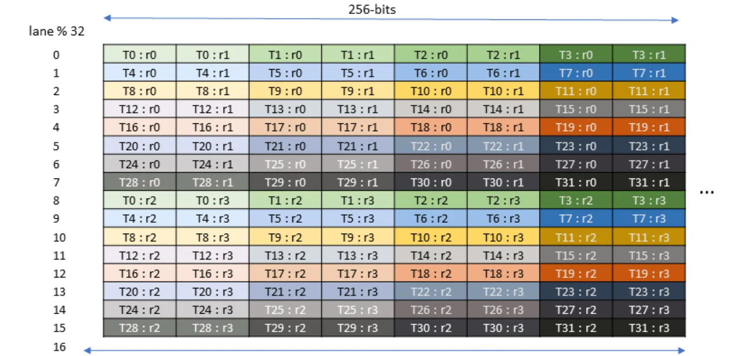
This instruction is pretty complicated, but let’s break it down. If we look at the documentation on how the data is stored in tensor memory, we observe that tensor memory holds a 64x64 C_tile . The layout organization and access pattern, according to Figure 215 in NVIDIA’s Parallel Thread Execution ISA Version 9.0, is as follows:
So to access the memory, each warp in our launched block will need to read out 16 lanes, and the entire warp-group (4 warps), reads out the 64 lanes. The parameters (datapaths and bits) specify this load pattern and tcgen05_ld dispatches the tcgen05.ld.16x256b instruction internally to load each set of lanes.
This means that each iteration, the threads will load 256 bits, or 8 elements (not 16, as if you recall from our first blog that we accumulate the results in FP32 to preserve accuracy, and each element is thereby stored in a 4 byte spot in tensor memory) across the columns of tensor memory, for BN/8 iterations. This means each one of 32 threads within the warp must hold 4 elements (see Figure 185).
Repeat this BN//8 = 8 times, and each thread now holds 32 elements of the tile in an array of registers. Once this is done, we know that we’re successfully transferred all the data into our registers, and, de-allocate the tensor memory that we allocated.
4 - Registers→ GMEM
In terms of code, here is where we are now:
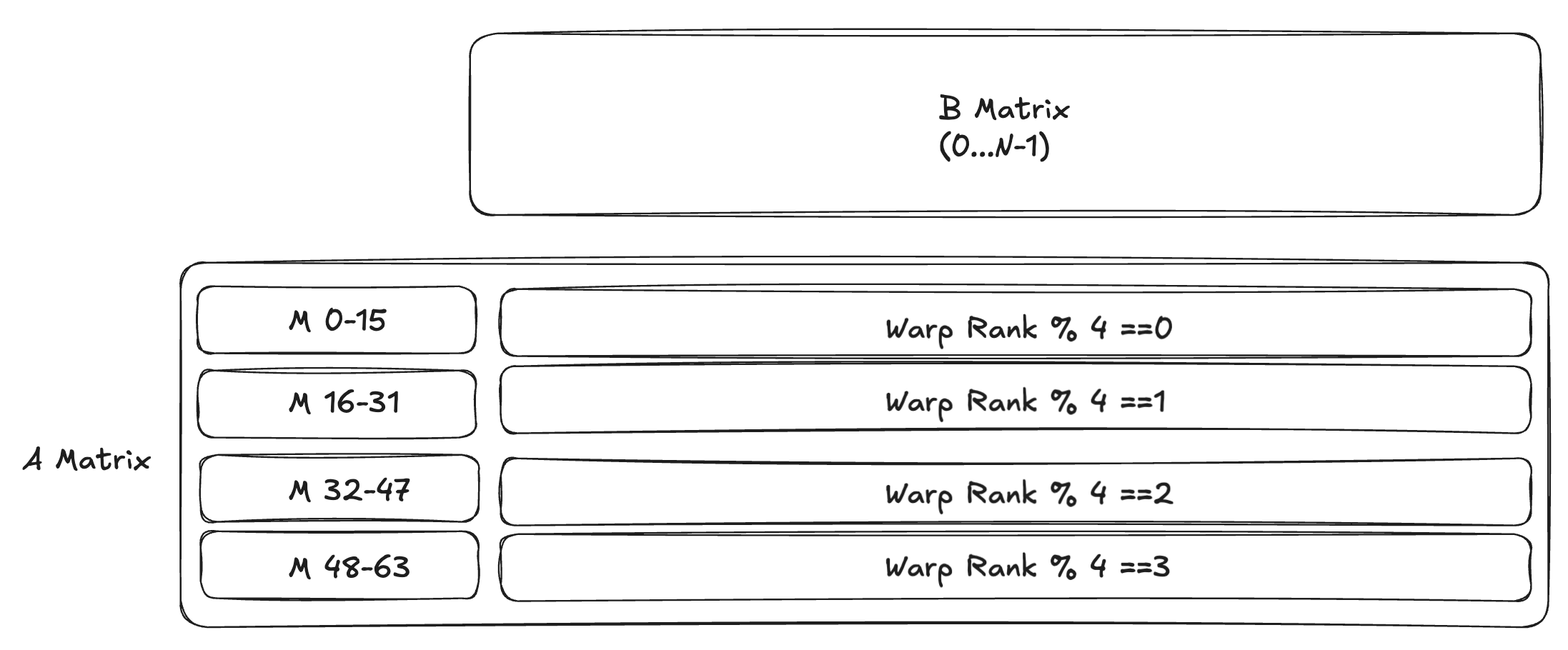
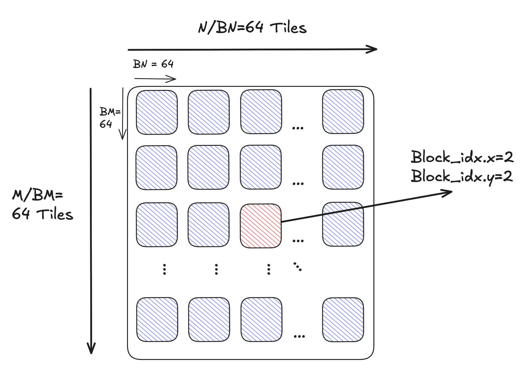
We’re still missing a key step: write_c_tile_to_global_memory, which moves the data from registers into global memory. To move the data, we begin by identifying where we want to write this data out to. Our matrix is 4096x4096. Each block is responsible for a 64x64 tile of this output. If we focus our attention on say block_idx.y = 2, block_idx.x = 2, this is responsible for outputting the 3rd tile of row 3:
We use the LayoutTensor.tile() method to extract a tile of the output matrix:
Then we further tile it for each warp:
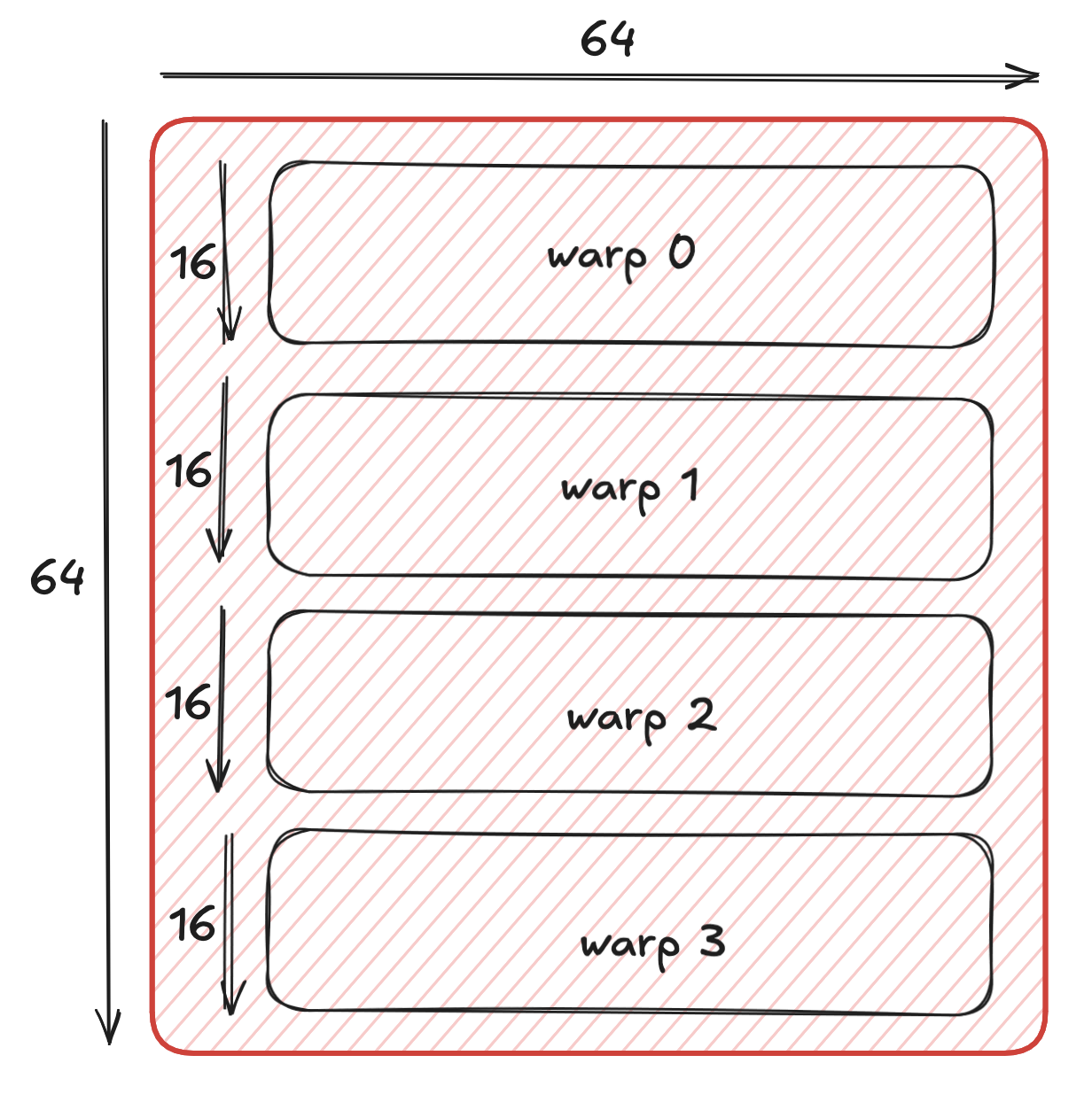
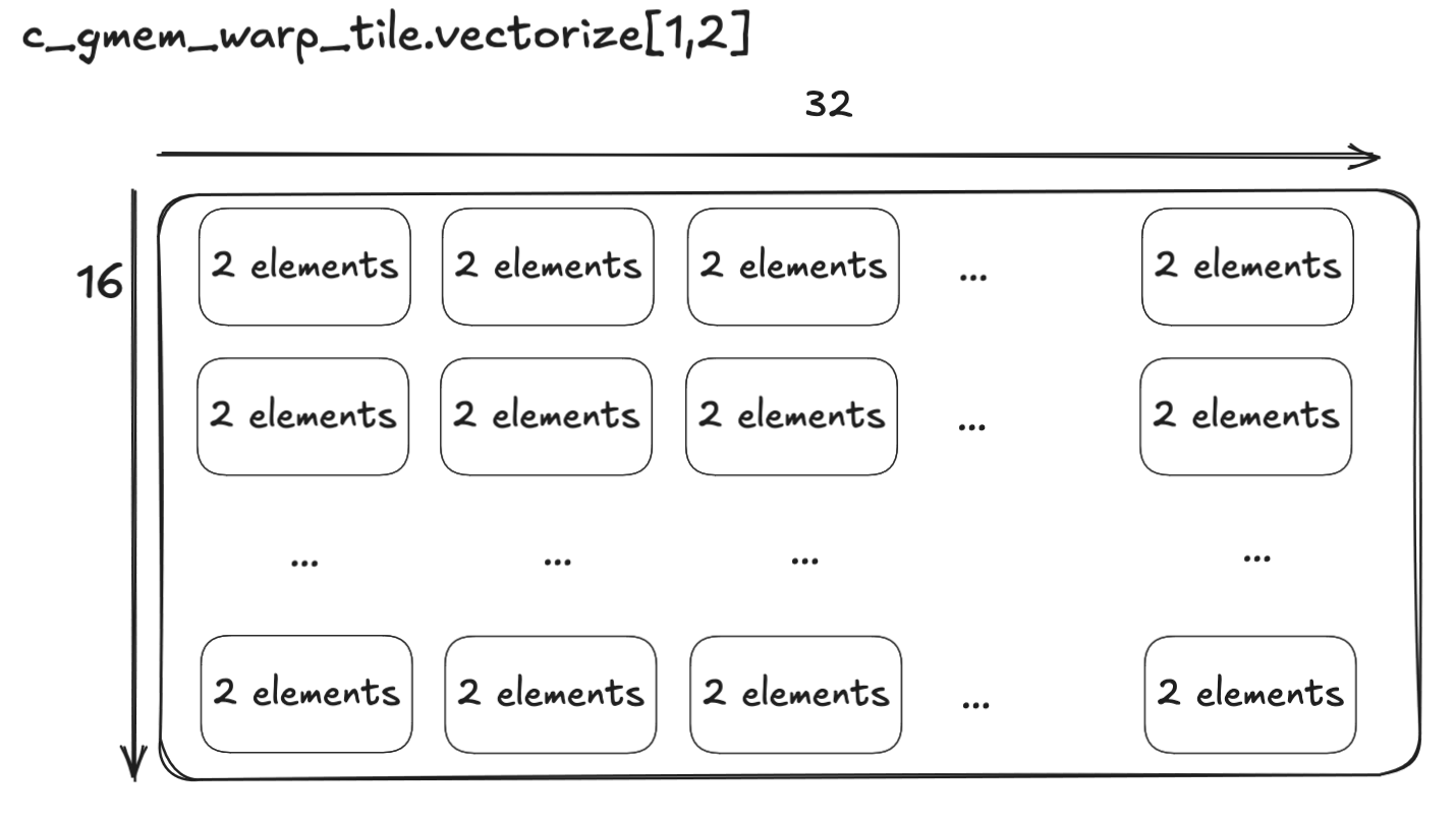
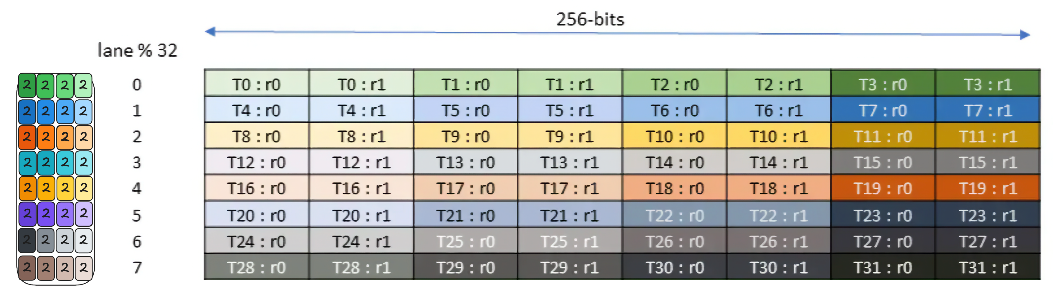
Let’s focus on the tile of warp 0, and how it will be affected. c_gmem_warp_tile of tile 0 represents the first 16 rows by 64 columns (16xBN) and we need to map this 16 by 64 tile to warp 0 since that is where the accumulator values are stored. The following plot shows how elements are mapped to lanes (threads) for the tcgen05.ld.16x256 PTX instruction:
There is quite some indexing involved. What if there was some way for us to create views—or little pockets—into the warp’s tile to give each thread a layout of exactly the pockets it needs to put its data into? Wouldn’t that be cool? If only we had a library function that did this. Mojo provides such a function, so this can be done succinctly:
This might be a bit complicated for folks who have just had their first look at LayoutTensor, so let’s visualize the view for thread 0. The first part of the code realizes that, since each thread stores 2 consecutive elements, the 16x64 tile can be viewed as a 16x32 tile of 2-value vectors each:
This is followed by .distribute[Layout.row_major(8, 4)] which distributes the 16x32 vectors over 8x4 threads repeatedly as demonstrated below.
The offset is calculated as row_major(8, 4)(lane_id()). For example, thread 0 gets the vector at (0, 0) in all the sub-matrices (green cell) and thread 6 gets the vector at (1, 3) similarly (blue cells in the figure below). In fact, each submatrix maps identically to NVIDIA’s layout in Figure 185:
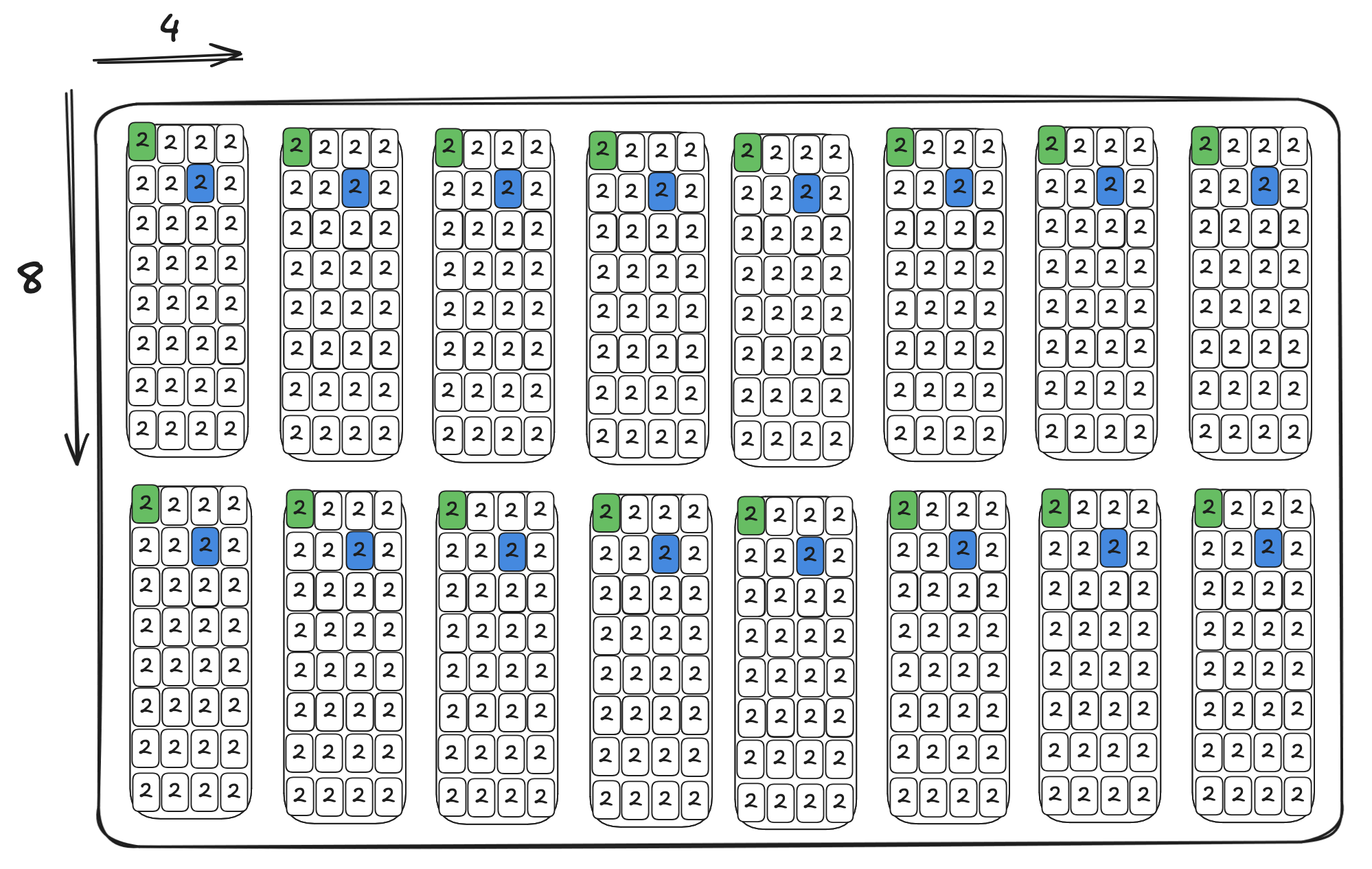
This results in 2x8 sub-matrices, each sub-matrix storing 8x4 2-value vectors. Furthermore, distribute gives each thread the view of the pockets it needs, just as we promised.
With this mapping, the output to global memory is trivially accomplished by a loop:
Using num_vecs_n, num_vecs_m=(8,2) as an example means that across each warp, we write out one sub-matrix at a time, first twice across the M dimension, then eight times across the N dimension. Here’s a quick overview of our loop in action:

The above is for a single warp. If we zoom out at the CTA level, we can map the CTA’s tile to the C matrix in global memory as follows:
5 - Setup shared memory for everything above
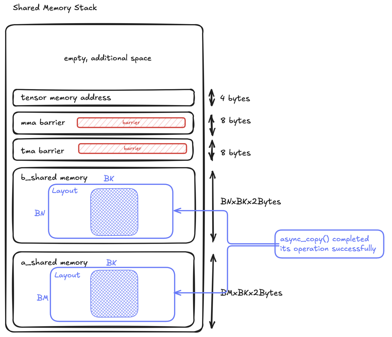
Before looking at how to setup the shared memory, let’s first examine what our shared memory stack looks like on the SM, which is the setup() phase we've skipped as far. We use shared memory primarily for the input tiles, memory barrier, and TMEM allocation.
The setup code above grabs the base address from dynamic shared memory allocation (external_memory), then grows the offset as shown below.
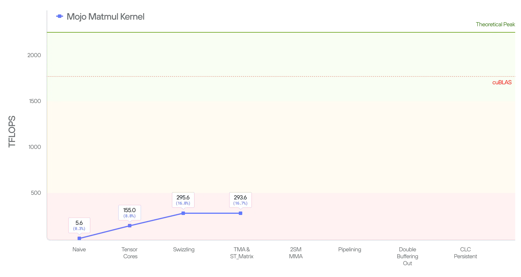
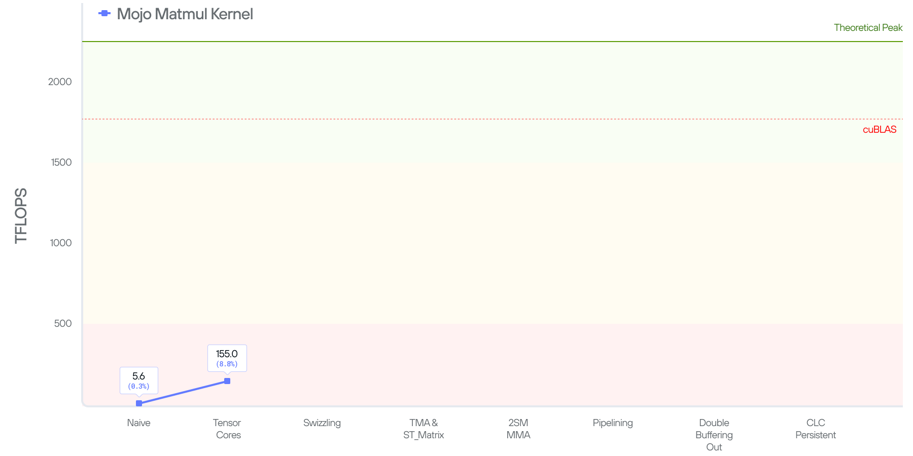
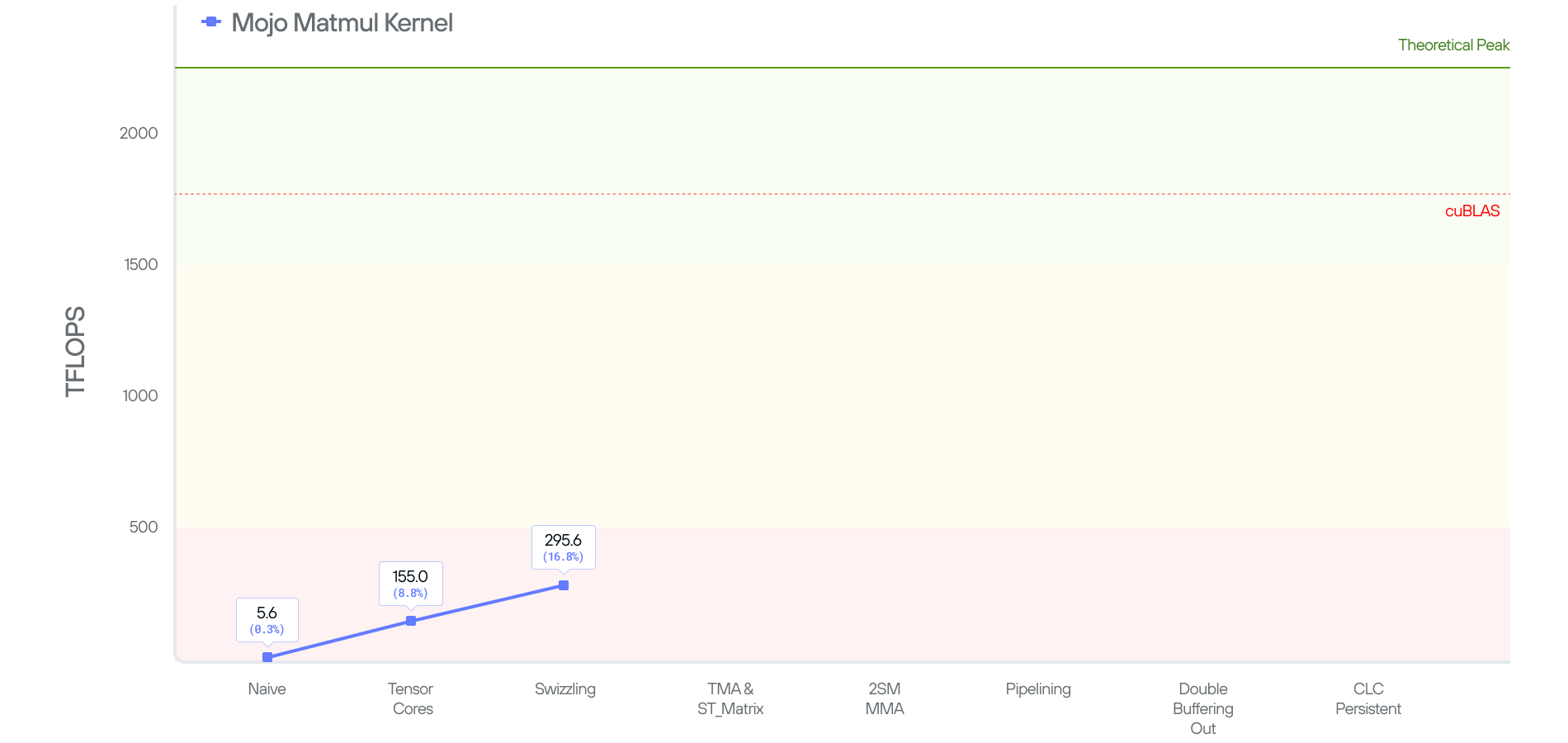
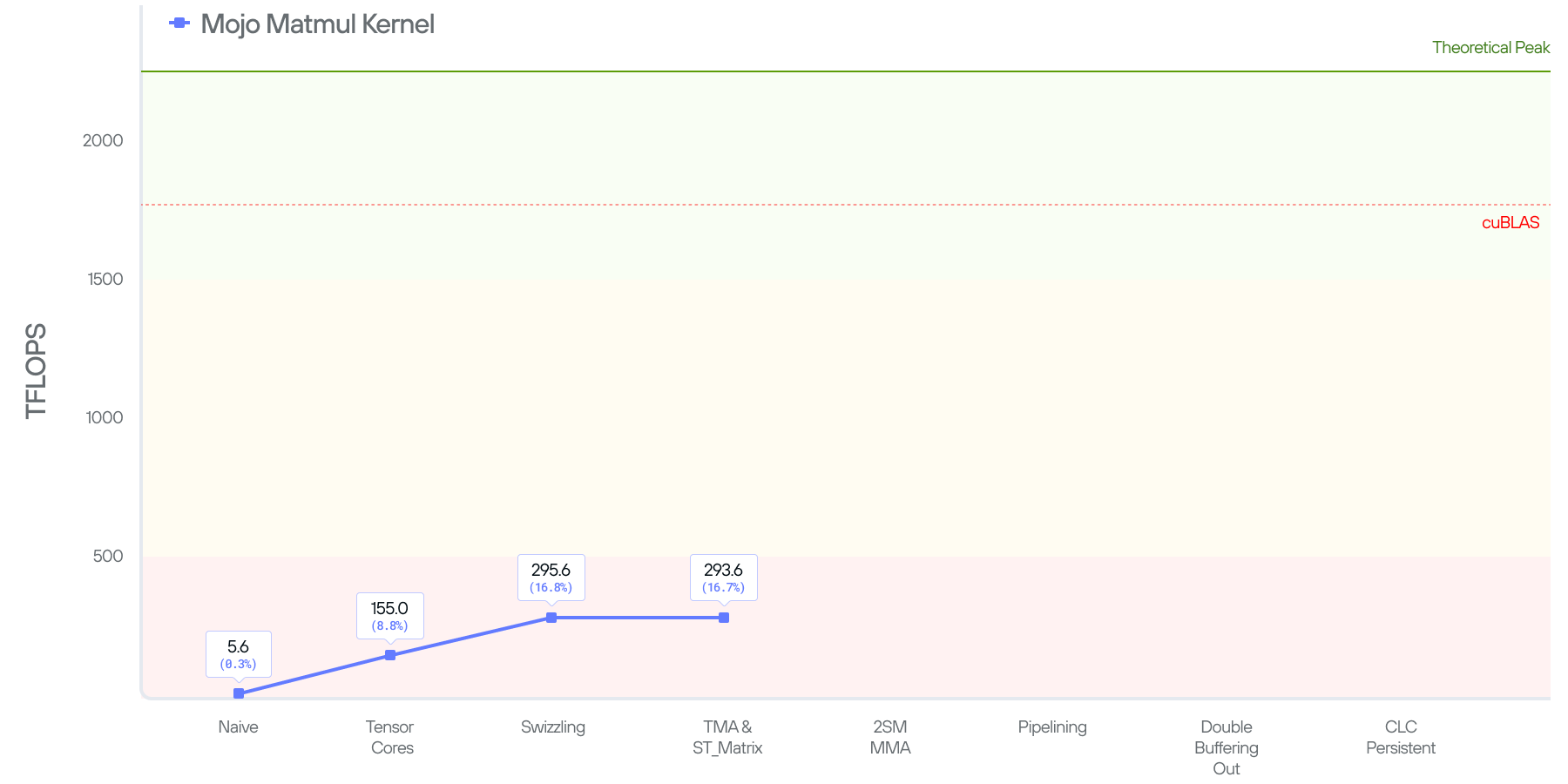
Putting things together, and benchmarking this kernel, we end up getting 155.0 TFLOPS, this is a 28x improvement over our naive kernel. But, to put things in perspective, the kernel is still operating at 8.7% of cuBLAS’ performance.
Kernel 3: swizzling
One overhead Kernel 2 has is launching multiple TMA calls for loading input tile. Recall that the reason we had to do that is because BK=64 , but the canonical layout needed by tensor core only allows us to copy 16B in K at a time. There are other layouts supporting larger K dimension per copy e.g. the widest 128B layout, which is best illustrated by CUTLASS’s comment:
The math indicates we indeed can use a single row-major tile BMxBK with BK = 64 (see 8T above) as long as we combine it with Swizzle<3, 4, 3> . What’s a swizzle? And why the magic pattern of <3, 4, 3>? To understand this better, let’s brush up our understanding of shared memory.
The code for kernel 3 is here.
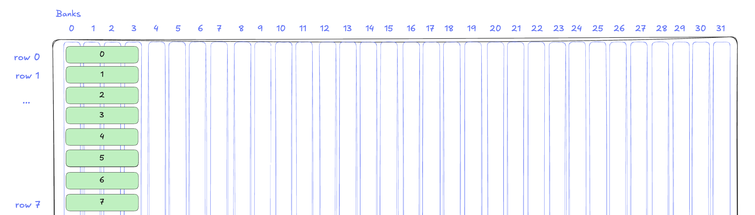
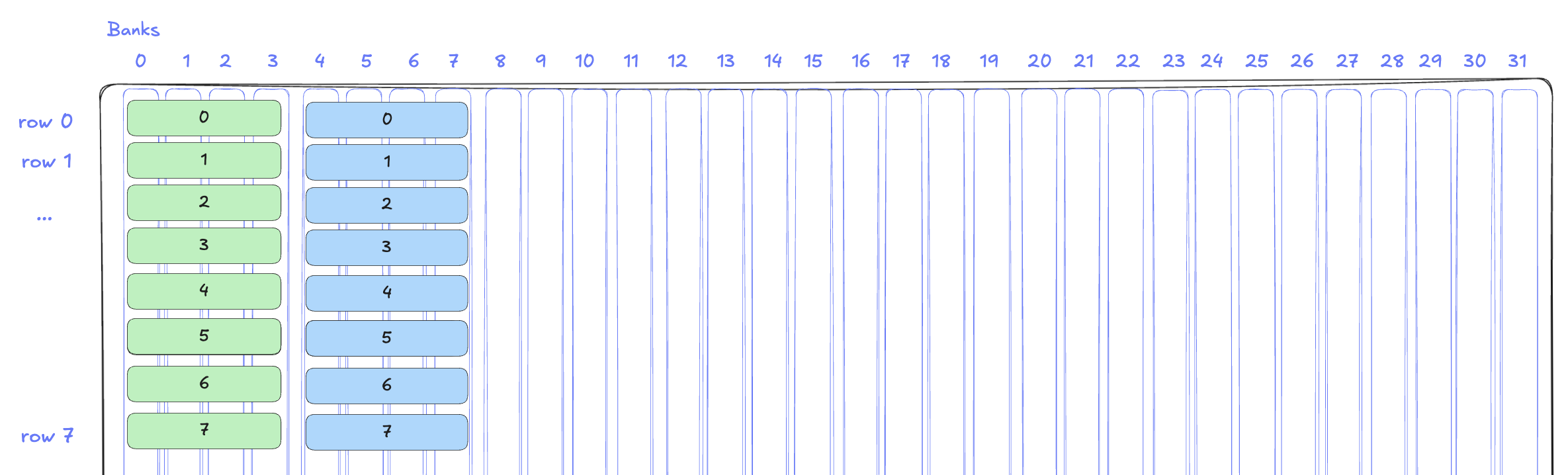
Shared Memory Banks
Shared memory consists of 32 consecutive 4B wide banks:
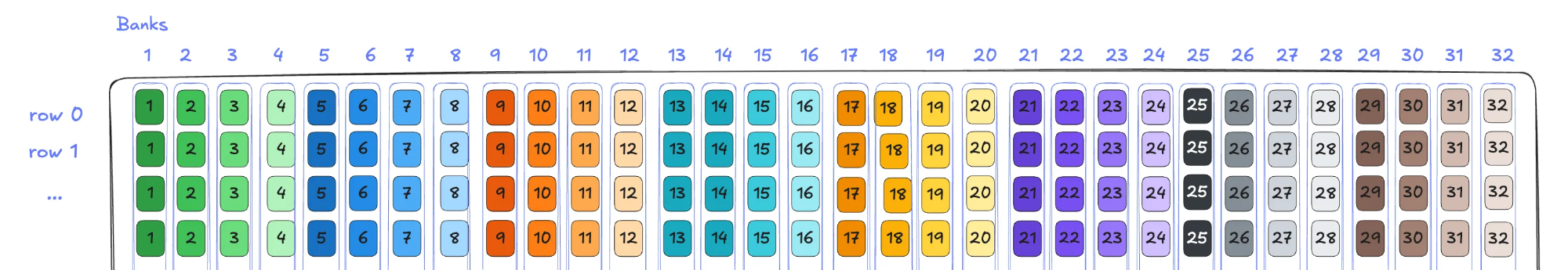
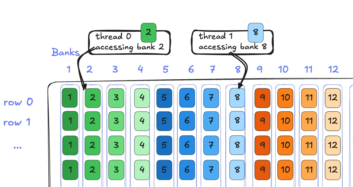
Each bank within the shared memory can service one request per cycle, and multiple threads accessing different banks within shared memory can all be serviced in the same cycle. That is, bank 0 services thread 0, and bank 16 services thread 1, at the same time:
Bank conflicts
However, what if two requests access the same bank? For example, consider the case where two threads access bank 0 for different addresses, say thread 1 now wanted to access the element at row 3 column 0.
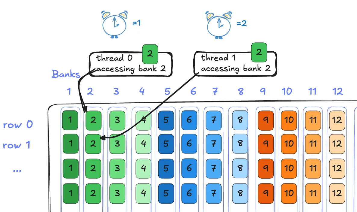
Now this takes 2 cycles. Bank 2 first services thread 0, and one cycle later, bank 2 services thread 1. Intuitively, this makes sense. To maximize throughput, the GPU is designed to load at most 128B per cycle by swiping all banks (32 banks times 4B per bank). A second load to the same bank needs to be scheduled in a later cycle.
Recall that the instructions are issued by warp. When threads within a warp try to access different addresses mapped to the same bank, the hardware has to break down the execution to multiple cycles. This stall in execution is called a bank conflict and obviously it's bad for performance .
If we apply the above to the 128B canonical layout (i.e. the tile is BMxBK and BK=64) then the first core matrix's 8 rows all mapped to same banks 0-3.
This would create an 8-way bank conflict per core matrix and cause the write for each row to happen sequentially. Obviously we need a technique to read the required data without the stalls created by bank conflicts.
Swizzling
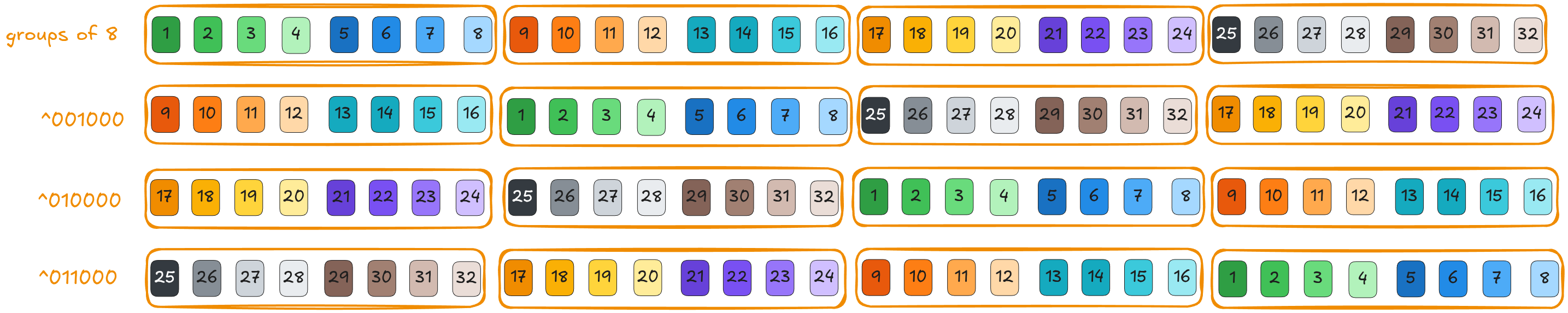
Swizzling is a technique to solve bank conflicts. Swizzling uses bitwise xor (^) to swap indices so that the data does not reside in the same bank. Let’s show swizzling via an example, let’s assume we have 16 banks for simplicity.
Row 0 stays the same by ^00:

Row 1: Flip adjacent pairs (0↔1, 2↔3, 4↔5, ...) by ^01:

Row 2: Flip pairs of pairs (01 ↔23, 45↔67) by ^10:

Row 3: invert every four values by ^11:

Note that the same index (1-16) on different rows have been swapped to different banks. That is, no bank conflict when threads access elements on different rows by the same index.
128 byte swizzling
Let's decipher the 128B swizzle pattern of <3, 4, 3>. The first 3 corresponds to 2^3 = 8: the number of rows in the core matrix. 4 maps to 2^4 = 16B (the width of the core matrix, 8 elements x 2B). The last 3 is 2^3 = 8, which implies 8 chunks of 16B span the entire 32 banks (128B). With these values, the swizzle function provides the correct xor pattern to resolve bank conflicts for core matrices. The pattern can be written in Mojo and generalized for common patterns. Visually it looks like:
Each 8 elements (16B = 8*2B) is grouped by zeroing 3 LSB in the xor operand. The xor computation swaps the groups within each row like we showed before. As a result, every 8 elements exist across different banks. And this continues as shown below:
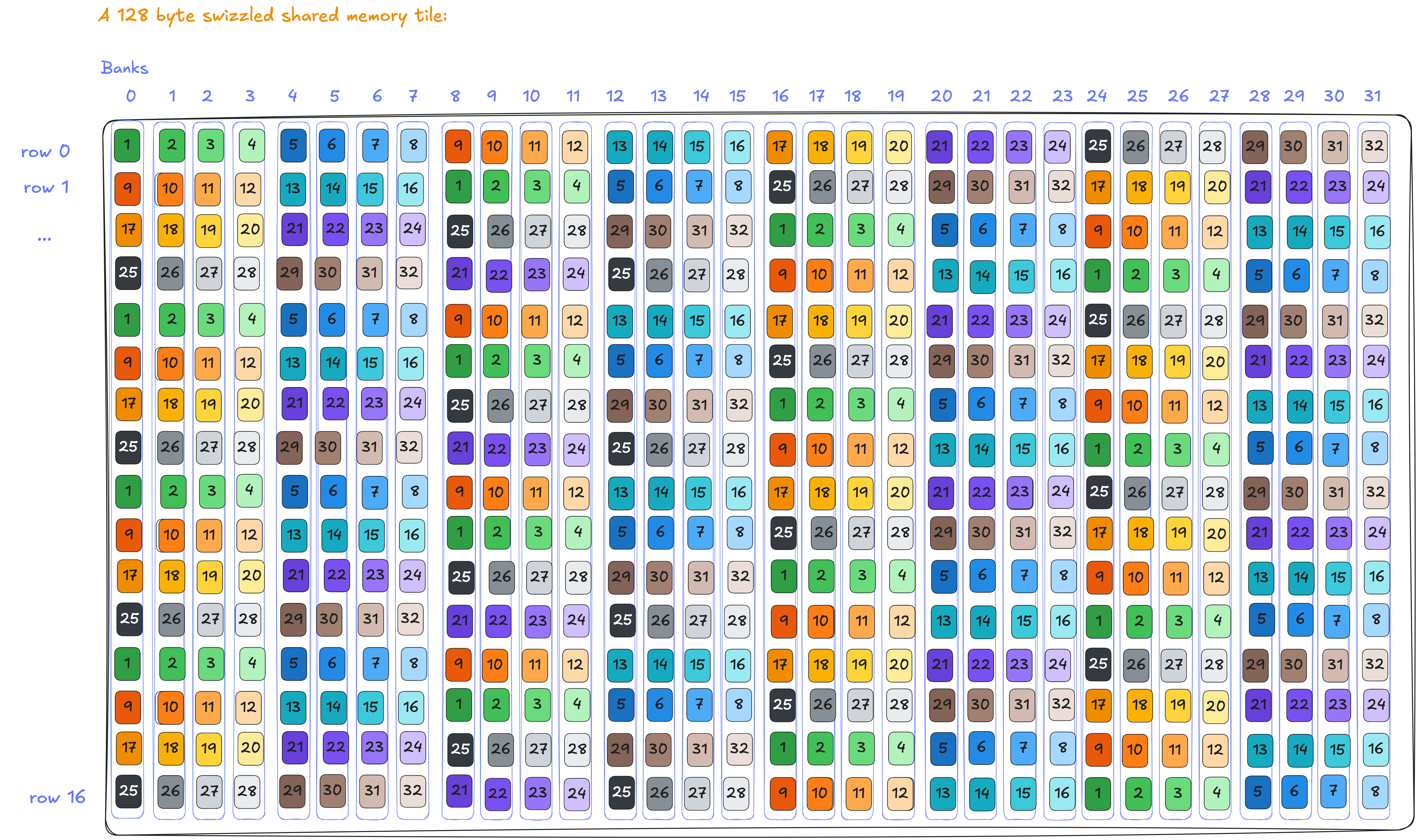
The full mathematical details are presented in the appendix. If we look at how two adjacent core matrices get swizzled onto 32 banks:
With the swizzle, the above becomes:
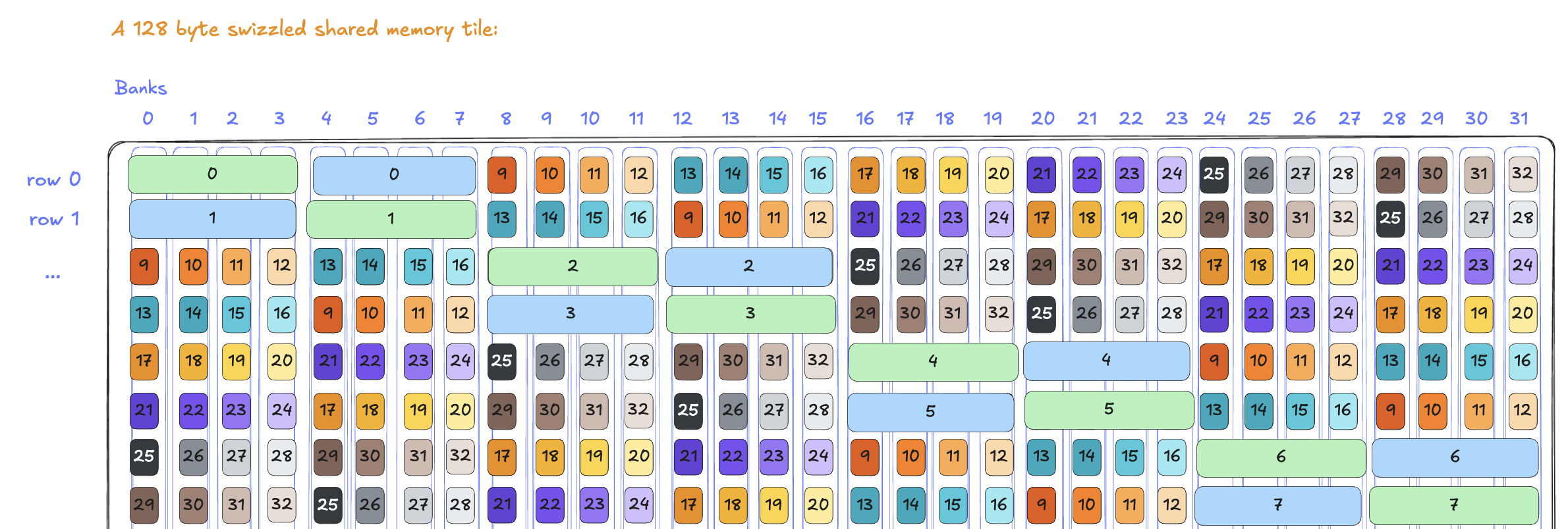
No two elements from the same core matrix ever end up in the same bank, because a core matrix has a width of 16 bytes and therefore no bank conflict with the 128 Byte swizzle.
🍭 This is why swizzling is extremely useful, and every high-performance GPU kernel will use it.
The updated kernel
The code changes for the kernel are minimal, since support for swizzling comes through the library’s layout tensors and instruction itself. The only code changes necessary is telling TMA and tcgen05.mma which swizzle mode to adopt:
Since LayoutTensor understands swizzling, we can hide the details of the swizzle operations behind the layout tensor API and leave our code unchanged.
Performance
With the above optimizations we are able to achieve 288.3 TFLOPs on B200 (an 87% improvement). In other words, the effects of shared memory bank conflicts basically cut our performance in half. And, by resolving the bank conflicts we are 16.4% of cuBLAS and quickly closing the gap.
Kernel 4: Packing output in shared memory and using TMA store
In the previous kernel's output, we write two contiguous BF16 values to global memory each time. That's only 4B per store, which is quite small given Blackwell can support up to 32B per store instruction (st.global.v8.b32). Moreover, we can use TMA to store an entire output tile per instruction to reduce the number of issued instructions. The code for kernel 4 is here.
Pack output in shared memory
To leverage TMA store, we need to pack the output data into shared memory. This is done by copying the registers to shared memory before loading the output from tensor memory to registers. Since the output in global memory is BF16, we must cast the registers from FP32 to BF16 before copying them to shared memory.
But, since the output result is fragmented by register in a particular layout (16x256 bits load, see TMEM->register section), we need to handle that when copying the registers to shared memory. Luckily, NVIDIA provides the stmatrix instructions to facilitate this step. The stmatrix instruction stores 8x16B core matrices distributed by the exact 16x256 bits layout to shared memory with the flexibility that users can specify the address in shared memory for each row. There appears to be a mismatch between 256 bits (32B) and 16B per row. This is because the data loaded from TMEM is in FP32 and we cast them to BF16 when storing to shared memory. The stmatrix instruction stores up to four core matrixes (2x2) per instruction. As a result, the packing of the 16x64 (BN=64) warp tile takes four iterations of stmatrix.
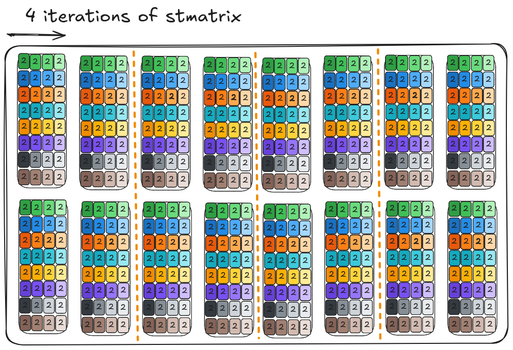
Note that this will hit bank conflict issue when loading into shared memory and as a result we use 128B swizzling (BN * 2B = 128B) to avoid the conflicts.
TMA store
With data swizzled and packed in shared memory, we can launch the TMA store operation to copy the data back to global memory asynchronously. The code below shows how the TMA store and how it handles the synchronization. Before the TMA issues the asynchronous store, we to fence the memory via fence_async_view_proxy to ensure previous packing in shared memory is visible to TMA store.
After issuing the TMA store, we first commit the stores using commit_group(). This groups the issued stores from the last commit up to that program counter. The following wait_group[N]() waits util only N groups of stores are still in flight. For instance, if there are 3 committed groups, wait_group[2]() ensures the first group is completed and the last two groups are in flight. In the above code, wait_group[2]() guards all TMA stores to finish. The ability to wait by commit groups allows to you to build pipelines and overlap other tasks efficiently in later optimizations.
There is another difference between the TMA store and the TMA load, since multiple threads can issue the TMA stores in parallel.
Here TMA_BN is based on the swizzling mode (e.g. TMA_BN=64 for 128B swizzling and BF16). If the tile dimension BN is greater, then we need to divide the dimension by TMA_BN and launch multiple TMA stores. For instance BN=128 maps to two stores as shown below, which are launched by two threads to maximize parallelism.
Performance
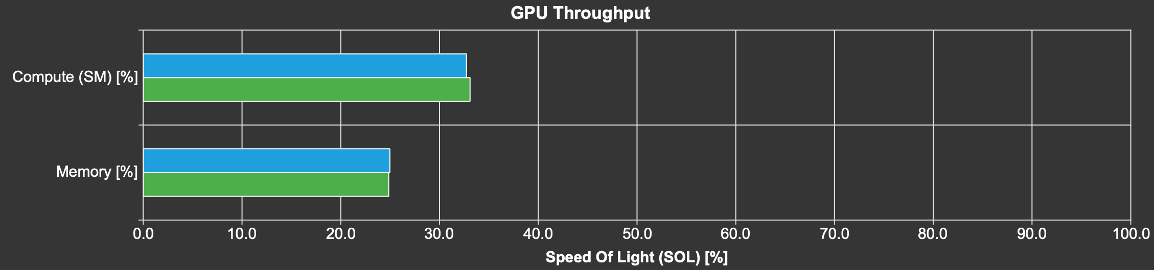
This kernel stays around the same at 293.6 TFLOPs, 0.7% slower to be exact. Why? Well, the performance is still fundamentally bound by global memory accesses.
The following plot shows the compute and memory throughput from NCU. The green bars are kernel 3 and the blue bars are kernel 4. As you can see, the compute and memory throughput are very low for both kernels.
Furthermore, the true power of TMA store lies in its asynchrony, which enables pipelining and overlapping operations. The current kernel sets the right ground work for us to leverage these features in subsequent posts.
In conclusion, in this post we demonstrated how to tile matmul and how to program a Blackwell GPU with the optimal instructions for performance using features such as TMA load/store, tcgen05.mma, stmaxtirx, etc. This effort results in a 58x improvement over the naive kernel, but still behind the performance of cuBLAS.
Future blog posts will build upon the kernel presented in this blog to improve the underlying schedule and algorithm of execution. Specifically, the next post will showcase how to build a warp specialized pipeline to overlap data transfer and computation to get performance that’s closer to state-of-the-art.
Appendix
Descriptors
tcgen05.mma uses descriptors to specify the input data’s layout in shared memory and instruction shape, data type, etc. To create an smem descriptors in Mojo one does:
adesc = MMASmemDescriptor.create[aSBO, aLBO, a_swizzle](a_smem_tile.ptr)
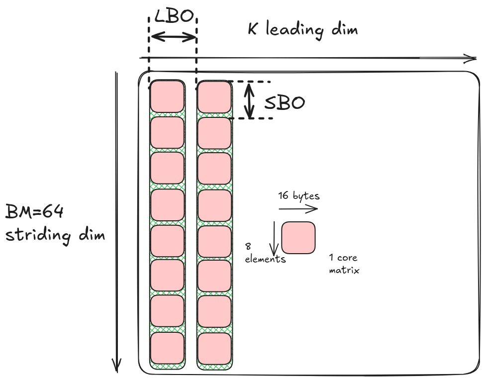
The MMASmemDescriptor takes care of encoding all this information in the format required by tcgen05.mma.The most important details areLBO and SBO:
- LBO (leading dimension byte offset): the number of bytes between two adjacent core matrices in K dimension.
- SBO (stride dimension byte offset): the number of bytes between two adjacent core matrices in the
M/Ndimension.
In kernel 2 i.e. without swizzling, printing this out for A shows:
As shown below, LBO is 1024B because the distance between two columns of core matrices is BM*16B = 1024B. SBO is 128B the size of each core matrix is 8x16B = 128B.
The UMMA descriptor idesc follows a similar pattern, except it’s 32 bits and encodes other information about the sparsity, data type, whether the matrices are transposed or not, and other information. We refer the readers to our source code for the detailed encoding.
Swizzling mathematics
The mathematical definition for swizzling is shown below. Given a swizzle defined as Swizzle(bits, base, shift):
If you look at the lower-level Mojo code, the swizzle is implemented as:
Consider the 128B swizzle where bits=3, base=4, and shift=3. The mathematics indicates we extracts 7-9 bits of the input address as a mask and xor the 4-6 bits with it, which generates the pattern shown in kernel 3:
Read all 4 parts of the "Matrix Multiplication on Blackwell" Series:
Part 2 - Using Hardware Features to Optimize Matmul
Part 3 - The Optimizations Behind 85% of SOTA Performance
Discover what Modular can do for you